
Page 159 - Microsensors, MEMS and Smart Devices - Gardner Varadhan and Awadelkarim
P. 159
SILICON FUSION BONDING 139
most of the common metals that are used in device fabrication melt below this temperature.
Therefore, to make full use of the potential provided by wafer bonding for microstruc-
tures, low-temperature bonding methods have to be developed. Attempts to lower bonding
temperatures and still achieve reasonable bond strength are currently under way.
Three annealing temperature ranges are of interest in wafer bonding:
1. Temperature less than 450°C for postmetallisation wafers.
2. Temperature less than 800 °C for wafers with diffusion dopant layers (e.g. p + etch-stop
layers).
3. Temperature greater than 1000°C for wafer bonding before processing. According to
the reaction mechanism, annealing at temperatures above 1000°C for several hours
should result in an almost complete reaction of the interface. A 1000 °C anneal for
about two hours gives sufficiently high bond strength for all subsequent treatments
(Harendt et al. 1991); it is not possible to separate the two bonded Si wafers without
breaking the silicon.
An 800 °C anneal results in sufficient bond strength for subsequent processes such as
grinding, polishing, or etching. However, the bonding is incomplete, as suggested by
partial delamination of thinned films after stress treatment (Harendt et al. 1991). The low-
temperature anneal (T < 450 °C) is inadequate for full wafer bonding. Although a signif-
icant increase in bond strength is already measurable after annealing at 200 °C (Kissinger
and Kissinger 1991), additional voids develop during annealing in the temperature range
200 to 700 °C and disappear at higher temperatures. If annealing is interrupted in this
temperature range, these voids remain after cooling; they probably originate from the inter-
facial water, which dissolves and reacts at temperatures above 800 °C. Patterned wafers,
however, have been successfully annealed at 450 °C without the development of additional
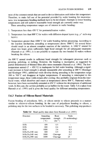
voids. In this case, the cavities probably act as buffers for the water. Table 5.4 is taken from
Harendt et al. (1991) and it gives the bond quality for different annealing temperatures.
5.6.3 Fusion of Silicon-Based Materials
Fusion bonding of poly silicon, SiO 2, or silicon nitride to silicon proceeds in a manner
similar to silicon-to-silicon bonding. In the case of polysilicon bonding to silicon, a
polishing step for the two surfaces to be bonded is necessary. This polishing step produces
Table 5.4 Bond quality data taken from Harendt et al. (1991)
Structure Annealing Bond Voids
temperature strength (% nonbonding)
–2
( °C) (Jm )
Si/Si 450 0.5 -
Si/Si 800 0.6 0.3
Si/Si 1000 2.6 0.3
Si/Si 3N 4(140 nm) 800 0.9 0.2
Si/Si 3N 4(140 nm) 1000 Cleavage 0.2
Si/Si 3N 4(300 nm) 1000 Cleavage 25