
Page 161 - Microsensors, MEMS and Smart Devices - Gardner Varadhan and Awadelkarim
P. 161
ANODIC BONDING 141
Top-chip:
Silicon bulk, 800 um thickness
Silicon oxide, 300 nm thickness
Pyrex#7740, 2.5 um thickness
Support-chip:
Surface layer (such as oxide,
nitride, poly-Si, or aluminum)
Silicon bulk, 380 um thickness
Figure 5.19 Top and support wafers used in a typical anodic bonding process (Hanneborg et al.
1992)
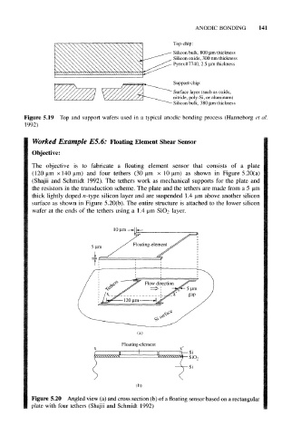
Worked Example E5.6: Floating Element Shear Sensor
Objective:
The objective is to fabricate a floating element sensor that consists of a plate
(120 um × 140 urn) and four tethers (30 urn x 10 urn) as shown in Figure 5.20(a)
(Shajii and Schmidt 1992). The tethers work as mechanical supports for the plate and
the resistors in the transduction scheme. The plate and the tethers are made from a 5 um
thick lightly doped n-type silicon layer and are suspended 1.4 um above another silicon
surface as shown in Figure 5.20(b). The entire structure is attached to the lower silicon
wafer at the ends of the tethers using a 1.4 um SiO2 layer.
10um-*|U—
(a)
Floating-element
(b)
Figure 5.20 Angled view (a) and cross section (b) of a floating sensor based on a rectangular
plate with four tethers (Shajii and Schmidt 1992)