
Page 160 - Microsensors, MEMS and Smart Devices - Gardner Varadhan and Awadelkarim
P. 160
140 SILICON MICROMACHINING: BULK
two smooth defect-free surfaces. The bonding mechanism is most probably identical to
silicon-to-silicon fusion bonding in that in both cases, Si—OH groups are present at the
surface. Thus, pretreatment (hydrophilisation) and annealing conditions are similar.
Because of the dissimilar mechanical characteristics of the different bonded materials,
the yield of void-free wafers can be significantly reduced by wafer bow or defects caused
by stress during thermal treatment. Bonding of wafers covered with a thin thermal oxide
or a thin silicon nitride results in homogenous bonded wafers, whereas oxides with thicker
oxide (or nitride) films develop voids during annealing (see Table 5.4).
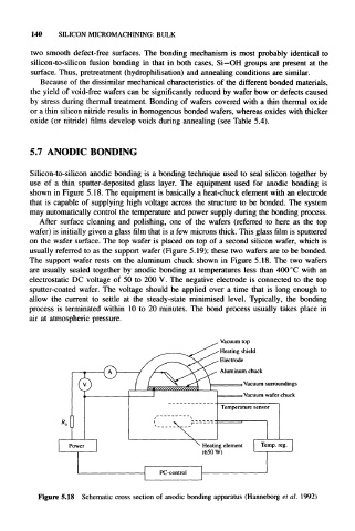
5.7 ANODIC BONDING
Silicon-to-silicon anodic bonding is a bonding technique used to seal silicon together by
use of a thin sputter-deposited glass layer. The equipment used for anodic bonding is
shown in Figure 5.18. The equipment is basically a heat-chuck element with an electrode
that is capable of supplying high voltage across the structure to be bonded. The system
may automatically control the temperature and power supply during the bonding process.
After surface cleaning and polishing, one of the wafers (referred to here as the top
wafer) is initially given a glass film that is a few microns thick. This glass film is sputtered
on the wafer surface. The top wafer is placed on top of a second silicon wafer, which is
usually referred to as the support wafer (Figure 5.19); these two wafers are to be bonded.
The support wafer rests on the aluminum chuck shown in Figure 5.18. The two wafers
are usually sealed together by anodic bonding at temperatures less than 400 °C with an
electrostatic DC voltage of 50 to 200 V. The negative electrode is connected to the top
sputter-coated wafer. The voltage should be applied over a time that is long enough to
allow the current to settle at the steady-state minimised level. Typically, the bonding
process is terminated within 10 to 20 minutes. The bond process usually takes place in
air at atmospheric pressure.
Vacuum top
Heating shield
Electrode
Aluminum chuck
Vacuum surroundings
Vacuum wafer chuck
Figure 5.18 Schematic cross section of anodic bonding apparatus (Hanneborg et al. 1992)