
Page 162 - Microsensors, MEMS and Smart Devices - Gardner Varadhan and Awadelkarim
P. 162
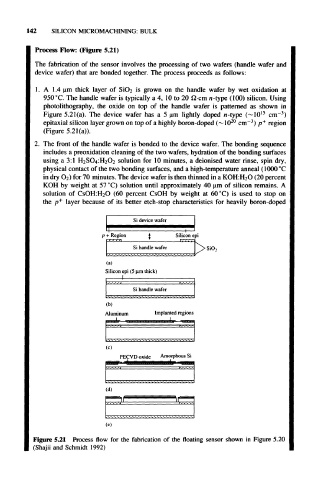
142   SILICON MICROMACHINING:  BULK


        Process Flow:  (Figure  5.21)
        The  fabrication  of  the  sensor  involves  the  processing  of  two  wafers (handle  wafer  and
        device  wafer) that  are bonded  together.  The process proceeds as follows:
        1.  A  1.4 urn  thick  layer  of  SiO 2  is  grown  on  the  handle  wafer  by  wet  oxidation  at
          950 °C. The handle  wafer is typically a 4,  10 to 20  £2-cm n-type  (100)  silicon.  Using
          photolithography,  the  oxide  on  top  of  the  handle  wafer  is  patterned  as  shown  in
                                                                           –3
          Figure  5.21(a).  The  device  wafer  has  a  5 urn  lightly  doped  n-type  (~10 15  cm )
                                                              20
                                                                   –3
          epitaxial  silicon  layer grown on top of a highly boron-doped  (~10  cm )  p +  region
          (Figure  5.21 (a)).
        2.  The  front  of  the handle wafer  is bonded  to  the  device wafer.  The  bonding  sequence
          includes a preoxidation cleaning of the two wafers, hydration of the bonding surfaces
          using  a  3:1 H 2SO 4:H 2O 2  solution for  10 minutes, a deionised  water rinse,  spin dry,
          physical contact of the two bonding surfaces, and a high-temperature anneal  (1000°C
          in dry O 2) for 70  minutes. The device wafer is then thinned in a KOH:H 2O (20 percent
          KOH  by  weight at  57 °C)  solution  until  approximately 40  um  of  silicon remains. A
          solution  of  CsOH:H 2O  (60  percent  CsOH  by  weight  at  60 °C)  is  used  to  stop  on
          the  p +  layer because  of  its  better  etch-stop  characteristics  for  heavily  boron-doped

                                   Si device wafer

                          p + Region           Silicon epi
                                   Si handle wafer
                            (a)
                           Silicon epi (5 um thick)

                                   Si handle wafer

                            (b)
                           Aluminum      Implanted regions


                            (c)
                               PECVD oxide  Amorphous Si


                           (d)


                           (e)

       Figure  5.21  Process  flow  for  the  fabrication  of  the  floating  sensor  shown in  Figure 5.20
       (Shajii  and  Schmidt 1992)