
Page 156 - Microsensors, MEMS and Smart Devices - Gardner Varadhan and Awadelkarim
P. 156
136 SILICON MICROMACHINING: BULK
a wafer stepper to expose the photoresist. The metal side-electrode is then transferred to
the metal by a metal RIE process. After the metal electrodes are patterned, the SiO 2 is
etched back with fluorocarbon-based RIE. Finally, the silicon mechanical structures are
released from the silicon substrate using an RIE process.
The SCREAM process described in the preceding text can be used to fabricate
complex, circular and triangular structures in SCS. These structures can include integrated,
high-aspect-ratio, and conformable capacitor actuators. The capacitor actuators are used
to generate electrostatic forces and so produce micromechanical motion.
Worked Example E5.5: Fabrication of Straight Cantilever Beam with Integ-
rated Aluminum Electrodes Using SCREAM
Objective:
To fabricate a free-standing cantilever beam 200 nm long, 0.8 um wide, and 3.5 urn
thick and coated with a 150 nm-thick SiO 2 layer (Zhang and McDonald 1992).
Process Flow:
The steps are based on the process shown in Figure 5.17, with the metal being aluminum.
1. The starting substrate is an arsenic-doped, 0.005 fi-cm, n-type (100) silicon wafer. A
layer of SiO 2 that is 400 nm thick is thermally grown on the substrate in a conven-
tional furnace in a steam O 2 ambient at 1100°C. The oxide is used as an etch mask.
The pattern to produce free-standing SCS structures is created using photolithography
in positive photoresist spun on the oxide layer on silicon. A wafer stepper is used
to expose the photoresist. The minimum feature size of the SCS beam structures is
400 nm (see Figure 5.17(a)).
2. The photoresist pattern on the oxide is transferred to the oxide in a CHF 3/O 2 plasma
etch at flow rates of 30 seem 5 and 1 seem, a chamber pressure of 30 mTorr and a
DC self-bias of 470 V in a conventional parallel-plate RIE tool. The etch rate of the
oxide is 23 nm/min. The photoresist on top of the oxide is then stripped off by an
O2 plasma etch (Figure 5.17(b)).
3. The oxide is then transferred to the silicon substrate using a Cl 2/BCl 3/H 2 RIE
in a commercial RIE tool. Three etch steps are required to accomplish a deep
vertical silicon etch (Figure 5.17(c)). The parameters for these etch steps are given
in Table 5.3.
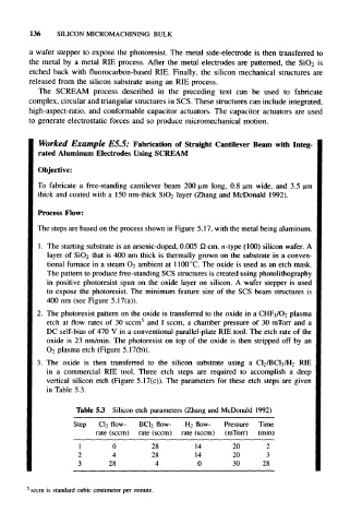
Table 5.3 Silicon etch parameters (Zhang and McDonald 1992)
Step C1 2 flow- BC1 2 flow- H 2 flow- Pressure Time
rate (sccm) rate (sccm) rate (sccm) (mTorr) (min)
1 0 28 14 20 2
2 4 28 14 20 3
3 28 4 0 30 28
1
sccm is standard cubic centimeter per minute.