
Page 152 - Microsensors, MEMS and Smart Devices - Gardner Varadhan and Awadelkarim
P. 152
132 SILICON MICROMACHINING: BULK
Worked Example E5.3: Formation of an Array of Thin Membranes
Objective:
The objective is to use electrochemical etching to fabricate an array of membranes with
thickness in the range 3 to 8 um and sides that are between 0.5 and 5 mm. The array is
to be fabricated on a p-type silicon substrate (Linden et al. 1989).
Process Flow:
1. The silicon wafers used are standard commercial, 280 um thick, (100)-oriented silicon
wafers. The wafers are boron-doped to a resistivity of 7 to 10 fi-cm, which corre-
–3
15
sponds to a doping concentration of approximately 1.5 x 10 cm . To produce a
p-n junction on the front surface of the wafer, a phosphorus-doped n-layer is diffused
on the p-type silicon wafer. The diffusion is performed by a predeposition, in which
oxygen is bubbled through a flask containing POCl 3, followed by a driven-in diffusion
with a mixed gas ambient of nitrogen and oxygen. Typical n-doping concentrations
–3
are around 10 17 cm .
2. Standard photolithographic methods are used to form a SiO 2 mask on the backside
(p-type side) of the wafer. The sides of the membranes range between 5 mm and
0.1 mm and the thickness (the thickness of the n-layers) range from 8 um down to
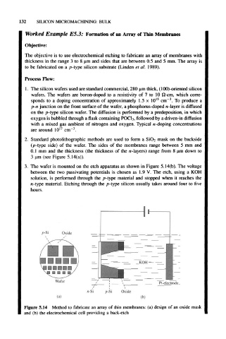
3 um (see Figure 5.14(a)).
3. The wafer is mounted on the etch apparatus as shown in Figure 5.14(b). The voltage
between the two passivating potentials is chosen as 1.9 V. The etch, using a KOH
solution, is performed through the p-type material and stopped when it reaches the
n-type material. Etching through the p-type silicon usually takes around four to five
hours.
Oxide
Wafer Pt-electrode.
n-Si
(a)
Figure 5.14 Method to fabricate an array of thin membranes: (a) design of an oxide mask
and (b) the electrochemical cell providing a back-etch