
Page 150 - Microsensors, MEMS and Smart Devices - Gardner Varadhan and Awadelkarim
P. 150
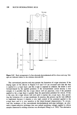
130    SILICON  MICROMACHINING:  BULK


                                                Op-amp


                    u             I •
                    06
                    o  0.4 "
                    f_\
                    1
                        on
                    » c  u.u
                    .c
                                Kb
                    i
                    |»  -0.4 -         Va
                    3
                      -0.8  -      h ™ -


     Figure  5.13  Basic arrangement of a four-electrode  electrochemical  cell for silicon etch-stop.  Volt-
     ages are indicated relative to the reference electrode  RE


       The  conventional  junction  etch-stop  permits  the  formation of n-type structures.  If the
     doping  types  of  the  silicon  in  Figures 5.12  and  5.13  are  reversed  such  that  the  bias
     is  applied  to  a  p-type  layer,  and  the  n-type  is  exposed  to  solution,  the  diode  is  now
     forward-biased  by  the  applied  potential.  If  the  forward-diode  current  density  is  low
     enough,  it  is  possible  that  the  n-type  silicon  will  not  passivate,  even  if  the  potential
     applied  to  the  p-type  layer  is  greater  than  the  passivation  potential  for  silicon. If this
     is  the  case,  the  n-type  silicon  will  etch  until  it  reaches  the  p-type  layer,  thus  permit-
     ting  the  formation  of  a  p-type  membrane. In  practice,  this  process  can  be  very  difficult
     to  implement  because  it  requires  a  very  tight  control  of  the  potential  applied  to  the
     p-type  layer  and  it  is  very  sensitive  to  the  diode-forward  characteristics.  To circum-
     vent  this  weakness  of  the  conventional  electrochemical  etch-stop  technique,  an  alter-
     native  dopant-selective technique  that  uses  pulsed anodising voltages  applied  to silicon
     samples immersed in etching solutions was developed  (Wang et al.  1992). This alternative