
Page 296 - Microsensors, MEMS and Smart Devices - Gardner Varadhan and Awadelkarim
P. 296
276 MICROSENSORS
Figure 8.42 Schematic layout of two types of magnetodiode: (a) fabricated by an SOI (sapphire)
process and (b) fabricated by a standard CMOS process. After Popovic et al. (1984)
\ yfy + \
c
/B
^ l
n+
n+
n
+
+
+
+
J
(a)
p-type 'B.
(b)
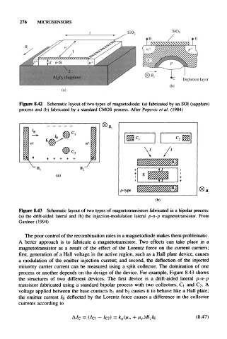
Figure 8.43 Schematic layout of two types of magnetotransistors fabricated in a bipolar process:
(a) the drift-aided lateral and (b) the injection-modulation lateral p-n-p magnetotransistor. From
Gardner (1994)
The poor control of the recombination rates in a magnetodiode makes them problematic.
A better approach is to fabricate a magnetotransistor. Two effects can take place in a
magnetotransistor as a result of the effect of the Lorentz force on the current carriers;
first, generation of a Hall voltage in the active region, such as a Hall plate device, causes
a modulation of the emitter injection current; and second, the deflection of the injected
minority carrier current can be measured using a split collector. The domination of one
process or another depends on the design of the device. For example, Figure 8.43 shows
the structures of two different devices. The first device is a drift-aided lateral p-n-p
transistor fabricated using a standard bipolar process with two collectors, C 1 and C 2. A
voltage applied between the base contacts b 1 and b 2 causes it to behave like a Hall plate;
the emitter current IE deflected by the Lorentz force causes a difference in the collector
currents according to
= (I C1 — (8.47)