
Page 295 - Microsensors, MEMS and Smart Devices - Gardner Varadhan and Awadelkarim
P. 295
MAGNETIC SENSORS 275
10 1
0 0.5 1.0 1.5
Magnetic flux density, B(T)
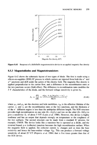
Figure 8.41 Response of a InSb/InSb magnetoresistive device to an applied magnetic flux density
8.5.3 Magnetodiodes and Magnetotransistors
Figure 8.42 shows the schematic layout of two types of diode. The first is made using a
+
silicon-on-sapphire (SOS) IC process in which carriers are injected from both the n and
+
p junctions and drift under the action of the electric field. The magnetic flux density is
applied perpendicular to the carrier flow, and a difference in the recombination rates at
the two junctions occurs (Suhl effect). The difference in recombination rates modifies the
I-V characteristics of the diode, and the forward voltage sensitivity is given by,
dV f
= •v; (8.46)
S v
dB
where ^ n and IJL P are the electron and hole mobilities, r eff is the effective lifetime of the
carrier, v\ and v 2 are the recombination rates at the two junctions, and the thickness d
–
of the n diffusion region is less than the ambipolar diffusion length. The SOS structure
provides high recombination on one side (Si—Al 2O 3) and low on the other (Si—SiO 2) to
give a sensitivity S v of about 5 V/T (Lutes et al. 1980). However, this device is highly
nonlinear and has an output that depends strongly on temperature or the roughness of
the two surfaces. The second structure can be made from a standard IC process, for
example, CMOS. The device looks like a transistor but is operated as a diode, and the
reversed biased p-n (collector) junction becomes the high recombination surface. When
the magnetic field is applied, the collector current I C changes and so does the base
resistivity and hence the base-emitter voltage V BE This can produce a forward voltage
sensitivity of about 25 V/T (Popovic et al. 1984) that is five times greater than that of
the SOS device.