
Page 297 - Microsensors, MEMS and Smart Devices - Gardner Varadhan and Awadelkarim
P. 297
MAGNETIC SENSORS 277
In the second device, the collectors are now outside the base pads and the Lorentz force
creates opposing Hall fields in the emitter and base areas. Therefore, the injected emitter
current is modulated differently and so is the current flowing through the collectors. The
second device has a higher sensitivity (7%/T) than the first device (0.5 to 5%/T).
A bipolar device can also be designed in which both processes occur. Figure 8.44(a)
shows a photograph of such a device together with a plot of the difference in the collector
current against magnetic flux density (Avram et al. 1998). The plot shows that, when in
a common-base configuration, the collector current difference of the magnetotransistor is
a linear function of the applied flux density, as predicted by Equation (8.46), and has a
sensitivity of about 250 uA/T.
Magnetotransistors, like magnetodiodes, can also be made from a standard lateral or
vertical CMOS or diffusion-channel MOS (DMOS) process, which has the advantage of
higher sensitivities. Interested readers are referred to Middelhoek and Audet (1989) for
further details. Despite the promise of these latter devices, the most successful commercial
device is the Hall effect IC, which is simple and inexpensive to process.
8.5.4 Acoustic Devices and SQUIDs
Although a Hall effect IC is of practical use in many situations, there is a general problem
of low sensitivity. One possible solution, that is rather attractive, is to use magnetic
microsensors based on a delay-line SAW device. Figure 8.45 shows the basic structure
of a SAW magnetic sensor (Hanna 1987).
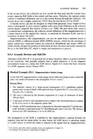
Worked Example E8.1: Magnetostrictive Strain Gauge
A thin film IDT magnetostrictive strain gauge can be fabricated using acoustic materials
17
and a wet metal etch-based on the propagation of Love waves .
Process Flow:
1. The substrate consists of a single-crystal nonmagnetic (111) gadolinium gallium
garnet wafer on top of which a thin epitaxial layer of garnet film (Y 1.5Lu 0.3Sm 0.3Ca 0.9
Ge 0.9Fe 4.1O 12) is grown.
2. This step is followed by the thermal evaporation of a layer of aluminum of about
100 nm thick.
3. A thin layer of ZnO is then sputtered down to improve the electromechanical coupling
of the Love waves to the magnetic garnet film.
18
4. Finally, an IDT metallisation layer is deposited by thermal evaporation and the elec-
trode structure is patterned using UV photolithography and a wet etch. The distance
between the IDT transducers is set to be 6000 um.
The propagation of the SAW is modified by the magnetoelastic coupling between the
magnetic spin and the strain fields. In other words, the SAW device is operating simply
as a strain sensor in which the strain is induced in the garnet film by magnetostriction.
17
Love waves, and other surface acoustic waves, are explained in Chapter 10.
18
An alternate lift-off process is described in Chapter 12.