
Page 79 - Multifunctional Photocatalytic Materials for Energy
P. 79
68 Multifunctional Photocatalytic Materials for Energy
range, that is, photon energy greater than the band gap of the semiconductor [87]. This
enhancement works suitably on metal oxide semiconductors with a trade-off between
the light absorption and charge carrier diffusion. In a representative photoelectrochem-
ical cell set up in Fig. 4.11C, hematite nanowire array grown in SPP Au hole array was
used as the photoanode for water splitting [91]. Ten-fold increase in the photocurrent
at 1.23 V versus RHE was achieved compared to hematite nanowire array photoanode
on bare FTO, which originates from both photonic and plasmonic energy transfer.
Photonic enhancement was demonstrated as coming from the SPP mode supported on
the Au hole array/hematite nanowire array, where under resonance, the incident light
was guided and concentrated into the hematite nanowire array above the band-edge of
hematite, which makes hematite nanowires act as an optical fiber to improve the light
absorption [91].
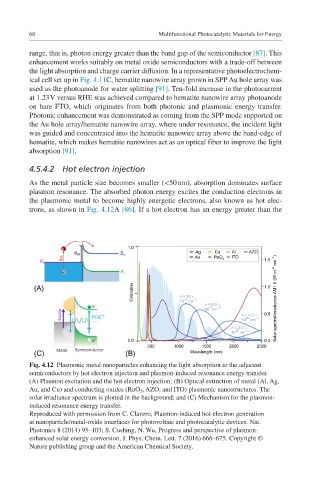
4.5.4.2 Hot electron injection
As the metal particle size becomes smaller (<50 nm), absorption dominates surface
plasmon resonance. The absorbed photon energy excites the conduction electrons in
the plasmonic metal to become highly energetic electrons, also known as hot elec-
trons, as shown in Fig. 4.12A [86]. If a hot electron has an energy greater than the
e – 1.0
j SB E C Ag Cu AI AZO
w Au RuO 2 ITO
– h 1.5
E F
h + E V
Extinction n = 10 ×
(A) 1.0
20
e – 10 cm –3 n = 8.0 × –3 Solar spectral irradiance AM1.5 (W m –2 nm –1 )
20
10 cm
Excite PIRET n = 4.0 × –3 0.5
20
10 cm
n = 2.0 ×
20
10 cm –3
h + 0.0 0.0
500 1000 1500 2000 2500
(C) Metal Semiconductor (B) Wavelength (nm)
Fig. 4.12 Plasmonic metal nanoparticles enhancing the light absorption to the adjacent
semiconductors by hot electron injection and plasmon-induced resonance energy transfer.
(A) Plasmon excitation and the hot electron injection; (B) Optical extinction of metal (Al, Ag,
Au, and Cu) and conducting oxides (RuO 2 , AZO, and ITO) plasmonic nanostructures. The
solar irradiance spectrum is plotted in the background; and (C) Mechanism for the plasmon-
induced resonance energy transfer.
Reproduced with permission from C. Clavero, Plasmon-induced hot-electron generation
at nanoparticle/metal-oxide interfaces for photovoltaic and photocatalytic devices. Nat.
Photonics 8 (2014) 95–103; S. Cushing, N. Wu, Progress and perspective of plasmon-
enhanced solar energy conversion, J. Phys. Chem. Lett. 7 (2016) 666–675. Copyright ©
Nature publishing group and the American Chemical Society.