
Page 76 - Multifunctional Photocatalytic Materials for Energy
P. 76
Energy band engineering of metal oxide for enhanced visible light absorption 65
O 2p co-contribute to the region of the VB, but the former is more negative than O
2p, which leads to a narrow band gap for the visible light absorption, while not in-
troducing the localized states between the VB and the CB (Fig. 4.9A) [53,72]. The
p-d repulsion has also been demonstrated to play a role in lifting the valence band of
a solid solution semiconductor, while keeping the conduction band unchanged and
thus reducing the band gap [74]. This phenomenon was observed in solid solution
semiconductors formed by ZnO and GaN. Both of them had band gaps greater than
3 eV, but their solid solutions absorbed light up to 500 nm [74]. More complicated
multiple metal cation oxides have also been attained in other solid solutions, such
as AgAl 1−x Ga x O 2 , Ca 1−x Bi x V x Mo 1−x O 4 , (AgNbO 3 ) 1−x (SrTiO 3 ) x , Cu 3x La 1−x Ta 7 O 19 , and
CuFe 1−x Cr x O 2 [75–79].
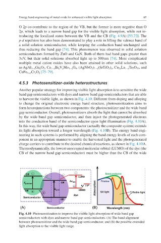
4.5.3 Photosensitizer-oxide heterostructures
Another popular strategy for improving visible light absorption is to sensitize the wide
band gap semiconductors with dyes and narrow band gap semiconductors that are able
to harvest the visible light, as shown in Fig. 4.10. Different from doping and alloying
to change the original electronic energy band structure, photosensitization aims to
form heterojunctions between two components: the photosensitizer and the wide band
gap semiconductor. Overall, photosensitizers absorb the light that cannot be absorbed
by the wide band gap semiconductor, and then inject the photogenerated electrons
into the conduction band of the semiconductor upon light illumination (Fig. 4.10A).
In this way, the wide band gap semiconductor (actually the composite system) extends
its light absorption toward a longer wavelength (Fig. 4.10B). The energy band engi-
neering in such systems is performed by aligning the band energy levels of each com-
ponent in an appropriate manner to enable the harvested light and the photogenerated
charge carriers to contribute to the desired chemical reactions, as shown in Fig. 4.10A.
Thermodynamically, the lowest unoccupied molecular orbital (LUMO) of the dye (the
CB of the narrow band gap semiconductor) must be higher than the CB of the wide
Fig. 4.10 Photosensitization to improve the visible light absorption of wide band gap
semiconductors with dyes and narrow band gap semiconductors. (A) The band alignment
between photosensitizer and the wide band gap semiconductor, and (B) the possible extended
light absorption to the visible light range.