
Page 78 - Multifunctional Photocatalytic Materials for Energy
P. 78
Energy band engineering of metal oxide for enhanced visible light absorption 67
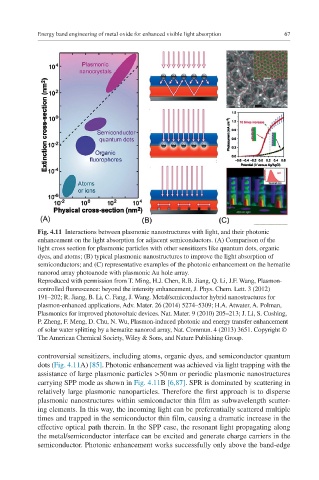
Fig. 4.11 Interactions between plasmonic nanostructures with light, and their photonic
enhancement on the light absorption for adjacent semiconductors. (A) Comparison of the
light cross section for plasmonic particles with other sensitizers like quantum dots, organic
dyes, and atoms; (B) typical plasmonic nanostructures to improve the light absorption of
semiconductors; and (C) representative examples of the photonic enhancement on the hematite
nanorod array photoanode with plasmonic Au hole array.
Reproduced with permission from T. Ming, H.J. Chen, R.B. Jiang, Q. Li, J.F. Wang, Plasmon-
controlled fluorescence: beyond the intensity enhancement, J. Phys. Chem. Lett. 3 (2012)
191–202; R. Jiang, B. Li, C. Fang, J. Wang. Metal/semiconductor hybrid nanostructures for
plasmon-enhanced applications, Adv. Mater. 26 (2014) 5274–5309; H.A. Atwater, A. Polman,
Plasmonics for improved photovoltaic devices. Nat. Mater. 9 (2010) 205–213; J. Li, S. Cushing,
P. Zheng, F. Meng, D. Chu, N. Wu, Plasmon-induced photonic and energy transfer enhancement
of solar water splitting by a hematite nanorod array, Nat. Commun. 4 (2013) 3651. Copyright ©
The American Chemical Society, Wiley & Sons, and Nature Publishing Group.
controversial sensitizers, including atoms, organic dyes, and semiconductor quantum
dots (Fig. 4.11A) [85]. Photonic enhancement was achieved via light trapping with the
assistance of large plasmonic particles >50 nm or periodic plasmonic nanostructures
carrying SPP mode as shown in Fig. 4.11B [6,87]. SPR is dominated by scattering in
relatively large plasmonic nanoparticles. Therefore the first approach is to disperse
plasmonic nanostructures within semiconductor thin film as subwavelength scatter-
ing elements. In this way, the incoming light can be preferentially scattered multiple
times and trapped in the semiconductor thin film, causing a dramatic increase in the
effective optical path therein. In the SPP case, the resonant light propagating along
the metal/semiconductor interface can be excited and generate charge carriers in the
semiconductor. Photonic enhancement works successfully only above the band-edge