
Page 73 - Multifunctional Photocatalytic Materials for Energy
P. 73
62 Multifunctional Photocatalytic Materials for Energy
from the aqueous electrolyte. Many attempts have been made to formulate such a
protective layer, but with little success for long-term stability. The most effective layer
so far is a multiple-layered film Al-doped ZnO (AZO)/TiO 2 by ALD with a thickness
greater than 200 nm [60]. Hydrogen evolution reaction (HER) co-catalysts, such as
Pt or MoS 2+x , layers could be further deposited to improve the current densities up
2
to nearly 8 mA/cm at 0 V versus RHE (pH = 4.9), as well as a Faraday efficiency of
nearly 100% for H 2 production [64–66].
Cu-based ternary oxides
This is a newly emerging family of ternary metal oxides, with the formula Cu x M y O z ,
that is alternative p-type semiconductors. A comprehensive review of this Cu-oxide
family is provided in Ref. 57. Different from Cu 2 O, in these ternary metal oxides,
10
the VB consists mainly of Cu 3d orbitals, whereas the CB predominantly consists
of d or s characters of the second metal M, which can accept the excited electrons
10
from the Cu 3d -based VB, and thus protect these ternary oxides from self-reduction
(Fig. 4.7) [57]. This family of p-type oxides has shown flexibility for tuning the band
gap by varying transition metals and the Cu(I) coordination environment, from as low
as ∼1.2 eV up to >3.0 eV (Fig. 4.7), which is able to cover a very broad sunlight spec-
trum. Because this oxide family emerged only recently, a significant amount of work
lies ahead to explore optoelectronic parameters such as charge carrier diffusion length.
4.5 Energy band engineering of metal oxides for
enhanced visible light absorption
The energy band structure determines a semiconductor's properties and of course has
significant influence on its photocatalytic performances. In terms of light absorption,
the band gap governs the absorption spectral range of a semiconductor and the theo-
retical maximum STC conversion efficiency. The electronic band structure also deter-
mines the nature of optical transition, as discussed in Section 4.2 in regard to direct
and indirect band gap semiconductors. In this section, we do a comprehensive review
of the approaches commonly used to engineer the electronic energy band structure in
order to improve the visible light absorption of metal oxide photocatalysts. To avoid
reiterating the detailed discussions in other related chapters, here we focus mainly on
energy band engineering to improve light absorption.
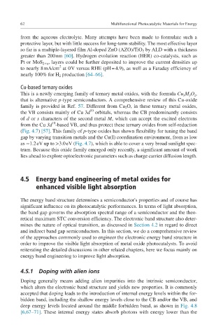
4.5.1 Doping with alien ions
Doping generally means adding alien impurities into the intrinsic semiconductor,
which alters the electronic band structure and yields new properties. It is commonly
accepted that doping leads to the introduction of internal energy levels within the for-
bidden band, including the shallow energy levels close to the CB and/or the VB, and
deep energy levels located around the middle forbidden band, as shown in Fig. 4.8
[6,67–71]. These internal energy states absorb photons with energy lower than the