
Page 490 - Book Hosokawa Nanoparticle Technology Handbook
P. 490
APPLICATIONS 10 DEVELOPMENT OF NOVEL FERROELECTRIC MATERIALS
planar dimensions. After heat treatment at 950 C for 24 1500
h in air, annealing under high-pressure oxygen at 35 1 MHz
MPa was performed at 750 C for 12 h to reduce oxy- 8000 1200
gen vacancies in the crystals. The composition of the a axis
crystals determined by inductively coupled plasma 6000 900
(ICP) emission spectrometry was Ba 0.75 Bi 8.32 Ti O , Dielectric permittivity (-) Dielectric permittivity (-)
27
7
which is a Ba-deficient and Bi-excess composition 4000 600
compared with the ideal one (BaBi Ti O ).
27
8
7
For electrical measurements, the crystals were cut so 2000 300
as to apply electric field along the a(b) directions c axis
according to the crystallographic axis determined by the 0 0
90 -domain structure. The small crystals of 300 400 500 600 700
3
1 0.2 0.25 mm (Au electrodes were sputtered on Temperature (°C)
2
1 0.2 mm faces) were used for polarization measure-
ments. Single crystals of BiT and BBTi were also grown Figure 10.3
separately, and their properties were compared with Temperature dependence of dielectric permittivity of
those of the BiT–BBTi crystals. BiT–BBTi single crystals (1 MHz).
3. Layered structure, dielectric and leakage current
properties of BiT–BBTi crystals by the dashed line in Fig. 10.2b. The thickness of the
constituent layers was approximately 1.5 and 2.0 nm,
Fig. 10.2a shows the - 2 XRD pattern of BiT–BBTi and these values are in good agreement with half the
single crystals. Apparent 00l reflections originating lattice parameters c of BiT and BBTi, respectively.
from the superlattice structure were observed. Fig. These results clearly indicate that the alternative
10.2b shows the transmission electron micrograph of superlattice stacking of m 3 and m 4 layers are
a BiT–BBTi crystal. Since the crystals were easily maintained not only in nanometer scale but also in a
damaged by electron beam irradiation, this wider-ranging area. In addition to the alternate stack-
photograph was taken within a few seconds. ing, a stacking fault along the c axis was observed
Fig. 10.2c shows a micrograph of the region enclosed
(m -3-4-3-4-3-3-4-).
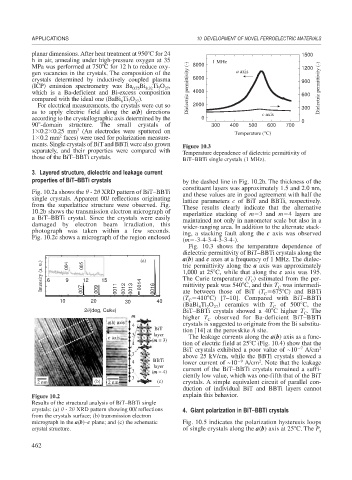
Fig. 10.3 shows the temperature dependence of
dielectric permittivity of BiT–BBTi crystals along the
a(b) and c axes at a frequency of 1 MHz. The dielec-
(a)
Intensity (a. u.) 6 9 004 12 15 0014 tric permittivity along the a axis was approximately
005
1,000 at 25 C, while that along the c axis was 195.
The Curie temperature (T ) estimated from the per-
C
mittivity peak was 540 C, and this T was intermedi-
0013
0012
0011
0016
007
009
C
ate between those of BiT (T 675 C) and BBTi
C
(T 410 C) [7–10]. Compared with BiT–BBTi
10 20 30 40 C
(BaBi Ti O ) ceramics with T C of 500 C, the
8
7
27
2 (deg, Cuk ) BiT–BBTi crystals showed a 40 C higher T . The
C
m higher T observed for Ba-deficient BiT–BBTi
a(b) axis C
4 crystals is suggested to originate from the Bi substitu-
BiT tion [14] at the perovskite A site.
3 layer
c axis (m = 3) The leakage currents along the a(b) axis as a func-
4 tion of electric field at 25 C (Fig. 10.4) show that the
BiT crystals exhibited a poor value of ~10 7 A/cm 2
3 above 25 kV/cm, while the BBTi crystals showed a
2
4 BBTi lower current of ~10 9 A/cm . Note that the leakage
layer
3 (m = 4) current of the BiT–BBTi crystals remained a suffi-
3 ciently low value, which was one-fifth that of the BiT
2 nm (b) 2 nm (c) crystals. A simple equivalent circuit of parallel con-
duction of individual BiT and BBTi layers cannot
Figure 10.2 explain this behavior.
Results of the structural analysis of BiT–BBTi single
crystals: (a) - 2 XRD pattern showing 00l reflections 4. Giant polarization in BiT–BBTi crystals
from the crystals surface; (b) transmission electron
micrograph in the a(b)–c plane; and (c) the schematic Fig. 10.5 indicates the polarization hysteresis loops
crystal structure. of single crystals along the a(b) axis at 25 C. The P
s
462