
Page 534 - Book Hosokawa Nanoparticle Technology Handbook
P. 534
APPLICATIONS 22 DEVELOPMENT OF PHOTONIC CRYSTALS
[2] Hosokawa Micron Cosmetics, Nanocrysphere on: [4] H. Tsujimoto: Development of functional skin and
http://www.nanocrysphere.com./lineup/index.html scalp care cosmetics using biodegradable PLGA
[3] H. Tsujimoto, K. Hara, C.C. Huang, T. Yokoyama, nanospheres, Drug Deliv. Syst., 21(4), 405–416
H. Yamamaoto, H. Takeuchi, Y. Kawashima, K. Akagi and (2006).
N. Miwa: Percutaneous absorption study of biodegradable [5] N. Miwa: Rejuvenation and Skin Protection, and
PLGA nano-spheres via human skin biopsies, J. Soc. Biotechonology (N. Miwa, Ed.), CMC Syutsupan,
Powder Technol. Jpn., 41 (12), 867–875 (2004). Tokyo, Japan (2003).
APPLICATION 22
22 DEVELOPMENT OF PHOTONIC CRYSTALS BASED ON NANOPARTICLE
ASSEMBLY
Photonic crystals are new types of optical materials, in
(a)
which small dielectric cells with the size of optical
wavelength (from several 100 nm to several 10 m)
are periodically arranged in two- or three-dimensions
[1, 2]. They are expected to contribute to the drastic
improvement of the performances of lasers and to the
miniaturization of integrated optical circuits. While
self-assembly techniques are extensively developed to
construct crystalline structures of nanoparticles, a very
different approach is introduced here: a method to
build up crystals by accurately arranging individual
nanoparticles by use of a micromanipulator under the
observation of a scanning electron microscope (SEM).
1. Nanoparticle assembly technique [3]
(b)
There are several techniques for assembling individual
small particles: such as micromanipulation under the
observation of an optical microscope, laser trapping,
and manipulation using a scanning probe microscope
[4]. Among them the micromanipulation under SEM
observation is the most suitable for three-dimensional
assembly of optical-wavelength-sized objects.
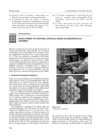
Fig. 22.1a illustrates an actual nanoparticle assembly
system. The system comprises of a field-emission-type
SEM coupled with a piezoelectric micromanipulator
[5]. An operator maneuvers the manipulator with joy-
sticks while observing a real-time SEM image with a
magnification from 5,000 to several tens of thousands.
Micro objects are stuck to a tip of a probe (needle) and
then transferred.
The manipulator is composed of a sample stage and Figure 22.1
a probe-positioning unit. The probe tip can be posi- Nanoparticle assembly.
tioned at an arbitrary point in a 15 mm cube on the
sample stage with an accuracy of 10 nm by means of a
unique coarse/fine positioning mechanism. The probe
is a glass needle made by drawing a heated glass cylin- the curvature of the probe tip, and the electron beam
der and then coating of Au. The adhesion forces acting condition (particularly, the acceleration voltage). The
on the object originate from electrostatic forces or van object can be reversibly picked up or deposited just by
der Waals forces [6, 7]. The magnitude of the adhesion proper movement of the probe in most cases [8].
forces strongly depends on the material combination, However, if necessary, a polymer film is coated on the
506