
Page 69 - Book Hosokawa Nanoparticle Technology Handbook
P. 69
FUNDAMENTALS CH. 1 BASIC PROPERTIES AND MEASURING METHODS OF NANOPARTICLES
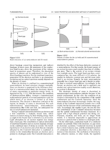
(a) Semiconductor (b) Metal
Conduction band
Energy Energy
Energy Band gap Energy
Valence band
D(E) D(E)
(a) Bulk semiconductor (b) Nanostructured semiconductor
D(E) D(E)
Figure 1.13.2
Figure 1.13.1 Density of states for the (a) bulk and (b) nanostructured
Band structures of (a) semiconductor and (b) metal. semiconductor particle.
direct bandgap conserving momentum and indirect shielded by the effect of the large dielectric constant of
bandgap. In most cases, the minimum of the conduc- a semiconductor. For that reason, the bound energy of
tion band locates above the maximum of the valence an exciton becomes much smaller than that of a hydro-
band in momentum space. Therefore, the absorption gen atom. That is, the activity of an exciton extends
spectra of photon can be understood in view of the over multiple atoms. The larger band gap that a semi-
direct bandgap transition. For the interband transition, conductor has, the more difficult it is to polarize, the
generation of the electron and hole is an elementary smaller its dielectric constant gets and the more stabi-
excitation and an optical spectrum mainly depends on lized is an exciton. Namely, an ionic semiconductor
the density of states. generally has a larger band gap and is harder to polar-
When an electron is confined in a nanostructured ize than a covalent semiconductor. Accordingly, in the
semiconductor, its band structure changes markedly. former, an electron and a hole tend to approach one
Since an electron is quantized in the thickness direc- another and, optical transition readily occurs; therefore,
tion in a nanostructured sheet, the electronic density an exciton is dominant.
of states concentrates at particular energy levels, as The electronic density of states is discretized in
depicted in Fig. 1.13.2. For that reason, the condition nanostructured semiconductor particles because of the
of photoexcitation differs. Assume a nanostructured spatial confinement. In that case, the condition of an
semiconductor particle of several nanometer scale for exciton is determined by the competition of the spatial
which travel of an electron is limited in all three confinement and the Coulomb interaction. Since the
dimensions. The electron is therefore confined in the semiconductor becomes increasingly smaller, the mag-
region; its density of states is discretized. For such nitude of the Coulomb interaction extends over a bulk
nanostructured semiconductors, semiconductor crystal, but the increase of the confinement energy pre-
nanoparticles like CdSe and ZnS, are anticipated for vails. Accordingly, the smaller it gets, the less the rela-
use as novel luminescent materials. tive contribution of the Coulomb interaction becomes
Strong Coulomb interaction between an electron and and the spatial confinement becomes dominant. In a
a hole establishes a mutually bound state, which region with a high obstacle potential and strong con-
reduces excitation energy by their binding energy. Such finement, electrons and holes are no longer freely
a couple in the bound state is referred to as an exciton. mobile. It is therefore impossible to approximate an
Light absorption by an exciton requires less energy exciton as a particle that is similar to a hydrogen atom.
than a band gap. The contribution to optical absorption On the other hand, conduction bands of a conductor
of interband transition and an exciton depends strongly (metal) are partially filled with electrons; no gap exists
on the combined states of atoms in crystals. The travel- in electronic excitation. Conducted electrons in metal
ing behavior of an electron and a hole that are mutually form a kind of plasma state, and the intraband transition
attracted by the Coulomb interaction is explained as of conduction electrons is described as the collective
similar to the relationship between an electron and a motion of free electrons. The oscillation of electrons by
proton in a hydrogen atom. The Coulomb interaction is this collective motion, in other words, the repetitive
46