
Page 106 - Nanotechnology an introduction
P. 106
8.3.1. Tip-Based Nanofabrication
The use of scanning probe microscopies (SPM) to characterize structure at the nanoscale suggests the reciprocal use of SPM-based methods to
generate such structure, that is, by picking up atoms from a store and placing them exactly where required, as was first proposed by Drexler [43]
(Figure 8.7).
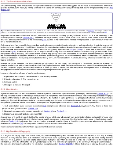
Figure 8.7 Illustration of tip-based nanofacture (in cross-section). Tip and substrate can move relative to each other. Each circle or disc corresponds to an atom (or superatom, see Section 8.3.2). The working tip is marked a. It can
engage in vertical interchange (of atoms a and b) and lateral interchange (of atoms b and c). Each of these concerted actions involves an intermediate state in which two or more atoms are simultaneously bonded to the tip [157].
Regardless of the chemical elements involved, the current molecular manufacturing paradigm involves tips—in fact it is the technology of the
scanning probe microscope (Section 5.1.1). Schweizer and Eigler's manipulation of xenon atoms on an ultracold nickel surface to form the letters
“IBM” was an iconic demonstration of the possibilities [151], but also of the extreme laboriousness of the procedure (it took almost 24 hours—and
had to be carried out at 4 K).
Curiously, advance has meanwhile been very slow, possibly because of a lack of long-term investment and clear direction, despite the large overall
funds spent on nanotechnology in the USA and elsewhere (too much funding has been allocated to incremental work with short-term goals). A more
recent landmark was the demonstration of atomic extraction using purely physical forces [130] and [131]—13 years after Schweizer and Eigler's
demonstration [151]. Clearly this approach is still very much in its infancy. Even the issue of automatic control of the tip (Schweizer and Eigler
manipulated their tip manually), which would enable one to simply specify the desired coordinates of each atom, and which would also undertake
the necessary checks to ascertain whether each atom had been correctly placed, has received minimal attention. What has been undertaken is
extensive calculations, mainly using density functional theory (DFT), of mechanosynthetic reactions; the slowly advancing experimental work is
lagging far behind.
Although nanoscale miniature tools work extremely fast (typically in the GHz range), high throughput of nanofacture can only be achieved by
massive parallelization, which in turn is only feasible if the required tools can make themselves—this was also part of Feynman's original vision.
The IBM “Millipede” project, in which large numbers of SPM tips work in parallel, still falls many orders of magnitude short of achieving the
throughput that would be required for materials fabrication yielding macroscopic quantities.
In summary, the main challenges of mechanosynthesis are:
1. Experimental verification of the calculations of rudimentary processes;
2. Extension of work on C, Si to cover all atoms;
3. Software control;
4. Strategies to increase throughput.
8.3.2. Nanoblocks
Significant acceleration of mechanosynthesis could take place if “nanoblocks”—pre-assembled (possibly by self-assembly, Section 8.2.1) units
that may comprise dozens or hundreds (or more) atoms—are manipulated via bottom-to-bottom methods. This immediately increases throughput
(in terms of the volume of artifacts produced) by a factor n , the number of atoms per block. The principles of software control should remain
b
unchanged. The basic idea of nanoblocks is to retain the quality, specificity and individuality of quantum objects while having the relative ease of
manipulation (compared with individual atoms) of nanoparticles. Regarding the choice of blocks, there are three main possibilities:
1. Multi-atom clusters (also known as superatoms) [34]; examples are fullerenes (see Section 9.3), Al K and K As . Some of these have
3
13
7
properties analogous to an atom (Section 2.5);
2. Nanoparticles or nanorods prepared conventionally (Section 6.1 and Section 6.2);
3. Biopolymers, especially globular proteins or RNA.
An advantage of 1. and 3. are strict identity of the blocks, whereas with 2. one will generally have a distribution of sizes and possibly of some other
properties too. An advantage of 2. and 3. is that they can readily be prepared in large quantities (this is also true for some kinds of clusters, notably
fullerenes (Section 9.3). In all cases doping or modification is generally possible. Some of these blocks spontaneously self-assemble into regular
structures (superlattices) [34], but their greatest potential use is in bottom-to-bottom fabrication.
In some sense nanoblocks are the hardware equivalent of finite element analysis.
8.3.3. Dip Pen Nanolithography
At a length scale slightly larger than that of atoms, dip pen nanolithography (DPN) has been developed by Chad Mirkin as a way of placing
molecules in finely resolved zones of a substratum. The technique works by coating the scanning probe microscope tip with a weakly adherent
molecular ink (e.g., proteins, relatively weakly adhering to a hydrophilic tip). When it is desired to write, the tip is lowered to the vicinity of the
substratum, to which the affinity of the ink is much stronger, and the ink's molecules are transferred to the substratum through a water meniscus—
the molecules (“ink”) are transferred to the substratum by capillary action (Section 3.3) [88]. It follows that writing is strongly dependent on the