
Page 49 - Nanotechnology an introduction
P. 49
crystal faces (cf. Section 4.1.4).
Dynamic measurements are likely to become of increasing importance as process as well as structure also falls under the scrutiny of the
metrologist. In situ techniques are required here; rastering is also to be avoided.
Metrology of the nano/bio interface presents challenges of immense complexity, often requiring completely different approaches from those
developed for wholly inanimate systems.
Although the functional characterization of nanodevices (device performance) could be legitimately included under nanometrology, it is really too
vast and varied a field; selected aspects are considered in Chapter 7 and Chapter 10.
5.1. Topography
Methods can be divided into “contact” and “noncontact”. Microscopically, there is little ambiguity about the notion of contact but in the nanoscale
one is aware that the Born repulsion prevents atoms from moving arbitrarily close to each other. Hence, although the atomic force microscope
(AFM)—Section 5.1.1—is often considered to be a miniature, nanoscale stylus scanned over a sample the repulsion between the atoms of the
AFM tip and sample asperity is actually action at a distance, hence the method could equally well be classified as noncontact. Scanning near-field
optical microscopy (SNOM), although usually grouped with AFM because the instrumentation is very similar, uses a “light (optical) stylus”, for which
the notion of contact with the sample is even more tenuous.
5.1.1. Contact Methods
Stylus-based profilers have long been used by engineers to determine the surface roughness of objects. A sharp-pointed stylus equipped with
some means of determining its vertical displacement is simply dragged over the surface perpendicular to the surface plane. The vertical motions
(deflexions from a mean) of the stylus are considered to more or less faithfully mimic the surface topography, which is recorded through a position
transducer attached to the stylus. This device was being progressively miniaturized, and the ability to determine subnanometer vertical
displacement was achieved for the first time by the Topografiner, invented by scientists at the US National Standards Institute [173] This nanoscale
vertical resolution was achieved using the electron tunneling effect, a quantum phenomenon (given the existence of two levels having the same
energy, there is a finite probability for an electron occupying one of the energy levels to pass to the other one (if unoccupied), depending
exponentially on the spacial distance separating the levels). The current measured between an electrically conducting stylus and an electrically
conducting sample can therefore be converted into sample topography.
Another indispensable technological advance was the perfection of piezoelectric motion controllers in the (x, y) plane (i.e., that of the surface) and
in the z direction (perpendicular to the surface). The stylus could then be raster-scanned very close to the surface. A feedback circuit can be
arranged to appropriately adjust the z displacement required to keep the tunneling current constant. The perfected instrument was called the
scanning tunneling microscope (STM) [21]. The principle, of miniature styli moving over the sample surface and at each position returning some
information about topography, or friction, or chemical nature, etc., has meanwhile been vastly extended to cover dozens of different scanning probe
microscopies (SPM), as the family is called. The most important (in the sense of being the most widely used) is called the atomic force microscope
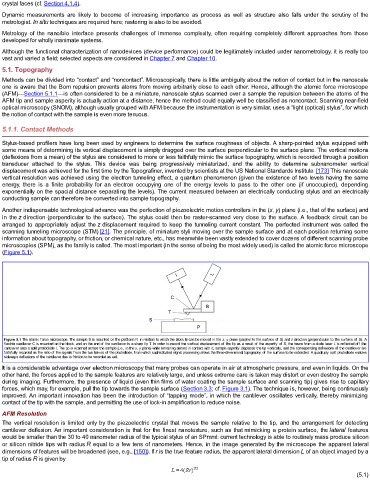
(Figure 5.1).
Figure 5.1 The atomic force microscope. The sample S is mounted on the platform P, in relation to which the block B can be moved in the x, y plane (parallel to the surface of S) and z direction (perpendicular to the surface of S). A
flexible cantilever C is mounted on the block, and on the end of the cantilever is a sharp tip T. In order to record the vertical displacement of the tip as a result of the asperity of S, the beam from a diode laser L is reflected off the
cantilever onto a split photodiode I. The tip is scanned across the sample (i.e., in the x, y plane) while remaining almost in contact with it; sample asperity displaces the tip vertically, and the corresponding deflexions of the cantilever are
faithfully recorded as the ratio of the signals from the two halves of the photodiode, from which sophisticated signal processing allows the three-dimensional topography of the surface to be extracted. A quadruply split photodiode enables
sideways deflexions of the cantilever due to friction to be recorded as well.
It is a considerable advantage over electron microscopy that many probes can operate in air at atmospheric pressure, and even in liquids. On the
other hand, the forces applied to the sample features are relatively large, and unless extreme care is taken may distort or even destroy the sample
during imaging. Furthermore, the presence of liquid (even thin films of water coating the sample surface and scanning tip) gives rise to capillary
forces, which may, for example, pull the tip towards the sample surface (Section 3.3; cf. Figure 3.1). The technique is, however, being continuously
improved. An important innovation has been the introduction of “tapping mode”, in which the cantilever oscillates vertically, thereby minimizing
contact of the tip with the sample, and permitting the use of lock-in amplification to reduce noise.
AFM Resolution
The vertical resolution is limited only by the piezoelectric crystal that moves the sample relative to the tip, and the arrangement for detecting
cantilever deflexion. An important consideration is that for the finest nanotexture, such as that mimicking a protein surface, the lateral features
would be smaller than the 30 to 40 nanometer radius of the typical stylus of an SPmml: current technology is able to routinely mass produce silicon
or silicon nitride tips with radius R equal to a few tens of nanometers. Hence, in the image generated by the microscope the apparent lateral
dimensions of features will be broadened (see, e.g., [150]). If r is the true feature radius, the apparent lateral dimension L of an object imaged by a
tip of radius R is given by
(5.1)