
Page 50 - Nanotechnology an introduction
P. 50
This problem can to some degree be overcome by independently measuring the precise shape of the tip (e.g., with a scanning electron
microscope) and then processing the deflexion profiles recorded using SPM in order to deconvolute the influence of tip shape—this is the exact
analogy of the modulation transfer function (MTF) approach used in optical image processing. Alternatively, finer styli (tips) can be used, for
example made by controlled etching of standard tips. Such tips enable subnanometer resolution to be obtained in principle. These ultrafine tips are,
however, very fragile and hence easily broken during scanning. Furthermore, if imaging in liquid, impurities dissolved in the liquid may rapidly
deposit on the tip. The effects on a conventional tip of R ~ 30 nm might be neglected, but such deposition is likely to significantly increase the
radius of an ultrafine tip. Carbon nanotubes (see Chapter 9), being extremely thin and rigid, offer a promising alternative to etched tips provided a
convenient way of manipulating and attaching them to the microscope cantilever, and possibly replacing them in situ when broken or contaminated,
can be found.
Contrast Enhancement
A significant challenge in the field is the metrology of fabricated surfaces, especially the characterization of chemical variegation. If only morphology
needs to be characterized, then the problem can be solved by either contact or noncontact techniques. The chemical contrast may, however, be
insufficient to yield a clear distinction between the different components. A practical approach to overcome this problem is selective post-
fabrication processing that only affects one of the components. This principle is applicable more widely than just to the imaging of complex
surfaces. For example, iron is a catalyst for carbon nanotube (CNT) growth using (plasma-enhanced) chemical vapor deposition, and hence if there
is a heterogeneous deposit (islands) of Fe on the surface, each island will serve as an initiator of columnar CNT formation.
When the variegation resides in differing organic functionalities, the contrast between regions of differing functionalities may be too low. In this
case, a useful technique may be to allow high contrast objects smaller than the smallest feature size to selectively bind to one functionality. Now that
a plethora of very small nanoparticles is available commercially, and others can be chemically synthesized by well-established methods (see, e.g.,
[135]), this method has become very useful and practicable. Examples of the decoration of block copolymer films are given in references [121] and
[109]. Using fairly extensive tabulations of single-substance surface tensions, the adhesive force between two substances in the presence and
absence of a fluid (in which the nanoparticles will usually be suspended) can be readily estimated (Section 3.2) and used to select a suitable
nanoparticle.
Scanning Ion Current Microscopy
A useful extension to the original SPM concept is scanning ion current microscopy (SICM) [62], in which the surface to be characterized is
immersed in electrolyte containing a counterelectrode, and the scanning probe is a miniature working electrode inside a very fine glass capillary
(Figure 5.2). The closer the end of the capillary is to the surface, the smaller the ion current, which can therefore be used to generate a map of the
topography. This method provides an innovative solution to the problem of excessive lateral force being applied to the sample and is particularly
useful for mechanically imaging ultrafragile samples, such as a living cell, since the capillary never comes into actual contact with the surface.
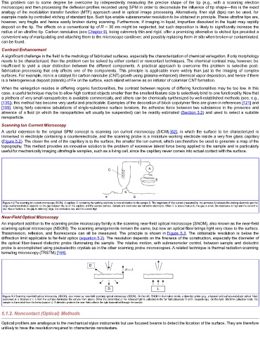
Figure 5.2 The scanning ion current microscope (SICM). A capillary C containing the working electrode is moved relative to the sample S. The magnitude of the current (measured by the ammeter A) between the working electrode and the
large counterelectrode E depends on the gap between the tip of the capillary and the sample surface. Sample and electrodes are bathed in electrolyte. When C is above feature b, the gap is small, the resistance is high and the current is
low. Above feature a, the gap is relatively large, the resistance low, and the current high.
Near-Field Optical Microscopy
An important addition to the scanning probe microscopy family is the scanning near-field optical microscope (SNOM), also known as the near-field
scanning optical microscope (NSOM). The scanning arrangements remain the same, but now an optical fiber brings light very close to the surface.
Transmission, reflexion, and fluorescence can all be measured. The principle is shown in Figure 5.3. The obtainable resolution is below the
diffraction limit applicable to far-field optics (equation 5.2). The resolution depends on the fineness of the construction, especially the diameter of
the optical fiber-based dielectric probe illuminating the sample. The relative motion, with subnanometer control, between sample and dielectric
probe is accomplished using piezoelectric crystals as in the other scanning probe microscopies. A related technique is thermal radiation scanning
tunneling microscopy (TRSTM) [166].
Figure 5.3 Scanning near-field optical microscopy (SNOM), also known as near-field scanning optical microscopy (NSOM). On the left, SNOM in illumination mode: a dielectric probe (e.g., a tapered and surface-metallized optical fiber)
positioned at a distance d ≪ λ from the surface illuminates the sample from above. Either the transmitted or the reflected light is collected in the far field (detectors D or D′, respectively). On the right, SNOM in collection mode: the
sample is illuminated from far below (source L). A dielectric probe in the near field collects the light transmitted through the sample.
5.1.2. Noncontact (Optical) Methods
Optical profilers are analogous to the mechanical stylus instruments but use focused beams to detect the location of the surface. They are therefore
unlikely to have the resolution required to characterize nanotexture.