
Page 257 - Op Amps Design, Applications, and Troubleshooting
P. 257
Band Reject Filter 239
On either side of the center frequency, we can expect the signals to pass with a
voltage gain of nearly unity.
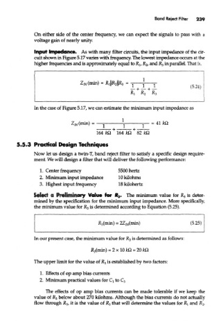
Input Impedance. As with many filter circuits, the input impedance of the cir-
cuit shown in Figure 5.17 varies with frequency. The lowest impedance occurs at the
higher frequencies and is approximately equal to RI, R& and R 3 in parallel That is,
In the case of Figure 5.17, we can estimate the minimum input impedance as
164 HI 164 kO. 82 fcO
5.5.3 Practical Design Techniques
Now let us design a twin-T, band reject filter to satisfy a specific design require-
ment. We will design a filter that will deliver the following performance:
1. Center frequency 5500 hertz
2. Minimum input impedance lOkilohms
3. Highest input frequency ISkilohertz
Select a Preliminary Value for H 3. The minimum value for R 3 is deter-
mined by the specification for the minimum input impedance. More specifically,
the minimum value for R 3 is determined according to Equation (5.25).
In our present case, the minimum value for R 3 is determined as follows:
R 3(min) = 2 x 10 fcQ = 20 ka
The upper limit for the value of R 3 is established by two factors:
1. Effects of op amp bias currents
2. Minimum practical values for Q to C 3
The effects of op amp bias currents can be made tolerable if we keep the
value of R 3 below about 270 kUohms. Although the bias currents do not actually
flow through jR 3, it is the value of R 3 that will determine the values for R l and R 2.