
Page 118 - Optical Communications Essentials
P. 118
Photodiodes and Receivers
108 Chapter Seven
In addition, the photodetector needs to
■ Be insensitive to temperature variations
■ Be compatible with the physical dimensions of the fiber
■ Have a reasonable cost compared to that of other system components
■ Have a long operating lifetime
Semiconductor-based photodiodes are the main devices that satisfy this set of
requirements. The two types of devices used are called a pin photodiode and an
avalanche photodiode (APD). This section addresses characteristics of pin photo-
diodes, and Sec. 7.2 discusses the APD.
7.1.1. Operation of a pin photodiode
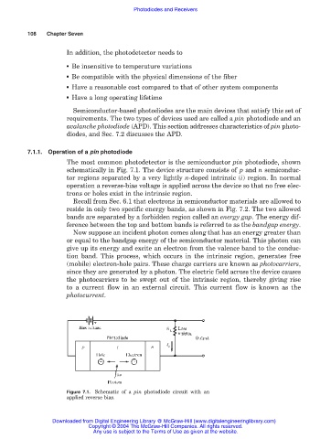
The most common photodetector is the semiconductor pin photodiode, shown
schematically in Fig. 7.1. The device structure consists of p and n semiconduc-
tor regions separated by a very lightly n-doped intrinsic (i) region. In normal
operation a reverse-bias voltage is applied across the device so that no free elec-
trons or holes exist in the intrinsic region.
Recall from Sec. 6.1 that electrons in semiconductor materials are allowed to
reside in only two specific energy bands, as shown in Fig. 7.2. The two allowed
bands are separated by a forbidden region called an energy gap. The energy dif-
ference between the top and bottom bands is referred to as the bandgap energy.
Now suppose an incident photon comes along that has an energy greater than
or equal to the bandgap energy of the semiconductor material. This photon can
give up its energy and excite an electron from the valence band to the conduc-
tion band. This process, which occurs in the intrinsic region, generates free
(mobile) electron-hole pairs. These charge carriers are known as photocarriers,
since they are generated by a photon. The electric field across the device causes
the photocarriers to be swept out of the intrinsic region, thereby giving rise
to a current flow in an external circuit. This current flow is known as the
photocurrent.
Figure 7.1. Schematic of a pin photodiode circuit with an
applied reverse bias.
Downloaded from Digital Engineering Library @ McGraw-Hill (www.digitalengineeringlibrary.com)
Copyright © 2004 The McGraw-Hill Companies. All rights reserved.
Any use is subject to the Terms of Use as given at the website.