
Page 123 - Optical Communications Essentials
P. 123
Photodiodes and Receivers
Photodiodes and Receivers 113
7.2. Avalanche Photodiodes
An avalanche photodiode (APD) internally multiplies the primary signal photo-
current before it enters the input circuitry of the following amplifier. The mul-
tiplication effect is achieved by applying a very high electric field across the
photodiode. When a photon-generated electron encounters this high electric
field, it can acquire sufficient energy to kick more electrons from the valence to
the conduction band, thereby creating secondary electron-hole pairs. These
secondary pairs also get accelerated to higher energies and therefore can gen-
erate even more electron-hole pairs. This increases receiver sensitivity since the
photocurrent is multiplied prior to encountering the electrical noise associated
with the receiver circuitry. The process is called avalanche multiplication, and
hence the device is called an avalanche photodiode.
Since the avalanche process is random, the mean number of electron-hole
pairs created is a measure of the carrier multiplication. This is called the gain
and is designated by M (or sometimes by G or G m ). The value of M can be made
quite large, but larger gains increase the noise currents of the device because of
larger variations in the photocurrent. Thus an APD has a noise figure F(M) that
is associated with the random nature of the avalanche process (see Sec. 7.4).
Analogous to the pin photodiode, the performance of an APD is characterized by
its responsivity R ADP . Thus in an APD the multiplied photocurrent I M is given by
P =
R
I M = R ADP 0 M P 0 (7.5)
where R is the unity-gain responsivity.
7.3. Comparisons of Photodetectors
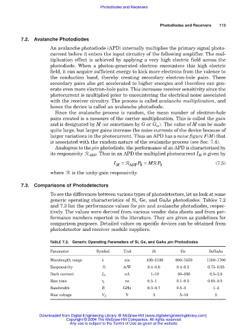
To see the differences between various types of photodetectors, let us look at some
generic operating characteristics of Si, Ge, and GaAs photodiodes. Tables 7.2
and 7.3 list the performance values for pin and avalanche photodiodes, respec-
tively. The values were derived from various vendor data sheets and from per-
formance numbers reported in the literature. They are given as guidelines for
comparison purposes. Detailed values on specific devices can be obtained from
photodetector and receiver module suppliers.
TABLE 7.2. Generic Operating Parameters of Si, Ge, and GaAs pin Photodiodes
Parameter Symbol Unit Si Ge InGaAs
Wavelength range λ nm 400–1100 800–1650 1100–1700
Responsivity R A/W 0.4–0.6 0.4–0.5 0.75–0.95
Dark current I D nA 1–10 50–500 0.5–2.0
Rise time τ r ns 0.5–1 0.1–0.5 0.05–0.5
Bandwidth B GHz 0.3–0.7 0.5–3 1–2
Bias voltage V B V 5 5–10 5
Downloaded from Digital Engineering Library @ McGraw-Hill (www.digitalengineeringlibrary.com)
Copyright © 2004 The McGraw-Hill Companies. All rights reserved.
Any use is subject to the Terms of Use as given at the website.