
Page 205 - Optofluidics Fundamentals, Devices, and Applications
P. 205
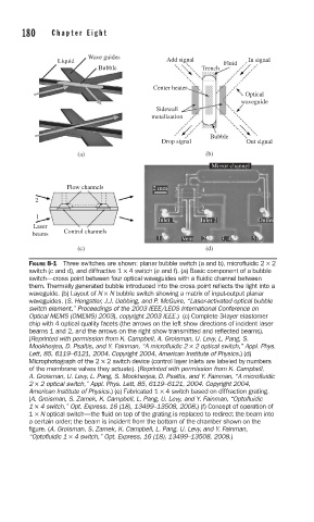
180     Cha pte r  Ei g h t


                         Wave guides
                 Liquid                      Add signal    Fluid  In signal
                            Bubble                    Trench
                                         Center heater
                                                                 Optical
                                                                waveguide
                                          Sidewall
                                         metalization

                                                        Bubble
                                           Drop signal           Out signal
                      (a)                              (b)
                                                        Mirror channel

                    Flow channels        2 mm  3      4             5
            2
                                              1       2
            1
                                           Inlet 1   Inlet 2        Outlet
           Laser
           beams   Control channels
                                          1      Vent  2   3, 4   5
                      (c)                              (d)
          FIGURE 8-1  Three switches are shown: planar bubble switch (a and b), microfl uidic 2 × 2
          switch (c and d), and diffractive 1 × 4 switch (e and f). (a) Basic component of a bubble
          switch—cross point between four optical waveguides with a fl uidic channel between
          them. Thermally generated bubble introduced into the cross point refl ects the light into a
          waveguide. (b) Layout of N × N bubble switch showing a matrix of input-output planar
          waveguides. (S. Hengstler, J.J. Uebbing, and P. McGuire, “Laser-activated optical bubble
          switch element,” Proceedings of the 2003 IEEE/LEOS International Conference on
          Optical MEMS (OMEMS) 2003), copyright 2003 IEEE.)  (c) Complete 3-layer elastomer
          chip with 4 optical quality facets (the arrows on the left show directions of incident laser
          beams 1 and 2, and the arrows on the right show transmitted and refl ected beams).
          (Reprinted with permission from K. Campbell, A. Groisman, U. Levy, L. Pang, S.
          Mookherjea, D. Psaltis, and Y. Fainman, “A microfl uidic 2 × 2 optical switch,” Appl. Phys.
          Lett, 85, 6119–6121, 2004. Copyright 2004, American Institute of Physics.) (d)
          Microphotograph of the 2 × 2 switch device (control layer inlets are labeled by numbers
          of the membrane valves they actuate). (Reprinted with permission from K. Campbell,
          A. Groisman, U. Levy, L. Pang, S. Mookherjea, D. Psaltis, and Y. Fainman, “A microfl uidic
          2 × 2 optical switch,” Appl. Phys. Lett, 85, 6119–6121, 2004. Copyright 2004,
          American Institute of Physics.) (e) Fabricated 1 × 4 switch based on diffraction grating.
          (A. Groisman, S. Zamek, K. Campbell, L. Pang, U. Levy, and Y. Fainman, “Optofl uidic
          1 × 4 switch,” Opt. Express, 16 (18), 13499–13508, 2008.) (f) Concept of operation of
          1 × N optical switch—the fl uid on top of the grating is replaced to redirect the beam into
          a certain order; the beam is incident from the bottom of the chamber shown on the
          fi gure. (A. Groisman, S. Zamek, K. Campbell, L. Pang, U. Levy, and Y. Fainman,
          “Optofl uidic 1 × 4 switch,” Opt. Express, 16 (18), 13499–13508, 2008.)