
Page 220 - Organic Electronics in Sensors and Biotechnology
P. 220
An Intr oduction to Or ganic Photodetectors 197
p n
(a)
– –
–
+ + + + +
+ + + +
+ –
– – – –
– – – – –
E c
+
E
+ + v
(b)
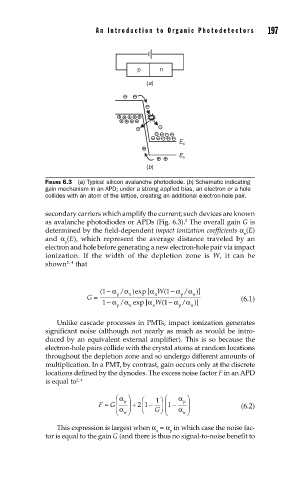
FIGURE 6.3 (a) Typical silicon avalanche photodiode. (b) Schematic indicating
gain mechanism in an APD; under a strong applied bias, an electron or a hole
collides with an atom of the lattice, creating an additional electron-hole pair.
secondary carriers which amplify the current; such devices are known
3
as avalanche photodiodes or APDs (Fig. 6.3). The overall gain G is
determined by the field-dependent impact ionization coefficients α (E)
n
and α (E), which represent the average distance traveled by an
p
electron and hole before generating a new electron-hole pair via impact
ionization. If the width of the depletion zone is W, it can be
2, 4
shown that
−
(1 − α / α )exp [α W(1 α / α )]
G = p n n p n (6.1)
1
1 − α / α exp [α W(1 −α / α )]
p n n p n
Unlike cascade processes in PMTs, impact ionization generates
significant noise (although not nearly as much as would be intro-
duced by an equivalent external amplifier). This is so because the
electron-hole pairs collide with the crystal atoms at random locations
throughout the depletion zone and so undergo different amounts of
multiplication. In a PMT, by contrast, gain occurs only at the discrete
locations defined by the dynodes. The excess noise factor F in an APD
is equal to 2, 4
⎛α ⎞ ⎛ ⎛ α ⎞
F = G ⎜ p ⎟ + 21 − ⎞ 1 ⎟ ⎜ 1 − p ⎟ (6.2)
⎜
⎝ α n⎠ ⎝ G⎠ ⎝ α n⎠
This expression is largest when α = α in which case the noise fac-
n p
tor is equal to the gain G (and there is thus no signal-to-noise benefit to