
Page 223 - Organic Electronics in Sensors and Biotechnology
P. 223
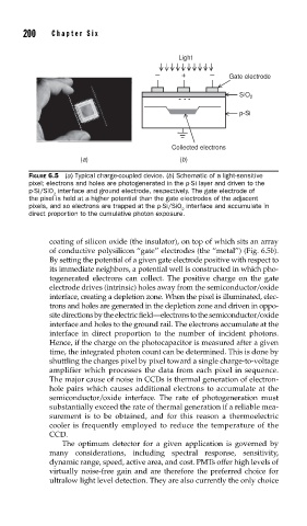
200    Cha pte r  S i x

                                                Light

                                          –      +      –    Gate electrode


                                                --             SiO 2
                                                 -
                                                               p-Si


                                              Collected electrons
                       (a)                      (b)

          FIGURE 6.5  (a) Typical charge-coupled device. (b) Schematic of a light-sensitive
          pixel; electrons and holes are photogenerated in the p-Si layer and driven to the
          p-Si/SiO  interface and ground electrode, respectively. The gate electrode of
                2
          the pixel is held at a higher potential than the gate electrodes of the adjacent
          pixels, and so electrons are trapped at the p-Si/SiO  interface and accumulate in
                                                 2
          direct proportion to the cumulative photon exposure.

               coating of silicon oxide (the insulator), on top of which sits an array
               of conductive polysilicon ‘‘gate’’ electrodes (the ‘‘metal’’) (Fig. 6.5b).
               By setting the potential of a given gate electrode positive with respect to
               its immediate neighbors, a potential well is constructed in which pho-
               togenerated electrons can collect. The positive charge on the gate
               electrode drives (intrinsic) holes away from the semiconductor/oxide
               interface, creating a depletion zone. When the pixel is illuminated, elec-
               trons and holes are generated in the depletion zone and driven in oppo-
               site directions by the electric field—electrons to the semiconductor/oxide
               interface and holes to the ground rail. The electrons accumulate at the
               interface in direct proportion to the number of incident photons.
               Hence, if the charge on the photocapacitor is measured after a given
               time, the integrated photon count can be determined. This is done by
               shuttling the charges pixel by pixel toward a single charge-to-voltage
               amplifier which processes the data from each pixel in sequence.
               The major cause of noise in CCDs is thermal generation of electron-
               hole pairs which causes additional electrons to accumulate at the
               semiconductor/oxide interface. The rate of photogeneration must
               substantially exceed the rate of thermal generation if a reliable mea-
               surement is to be obtained, and for this reason a thermoelectric
               cooler is frequently employed to reduce the temperature of the
               CCD.
                   The optimum detector for a given application is governed by
               many considerations, including spectral response, sensitivity,
               dynamic range, speed, active area, and cost. PMTs offer high levels of
               virtually noise-free gain and are therefore the preferred choice for
               ultralow light level detection. They are also currently the only choice