Page 46 - Organic Electronics in Sensors and Biotechnology
P. 46
Scaling Effects in Organic Transistors and Transistor-Based Chemical Sensors   23

               higher than the operating drain voltage (V , up to −5 V), which causes
                                                  ds
               the FET to operate in the linear region. The calculation of field-effect
               mobility derived from the transconductance of I  in the linear region
                                                        ds
                         2
               is 0.046 cm /(V⋅ s), and the on/off ratio (at V =−5 V) is 97 for this
                                                      ds
               device. The superlinear characteristics at the high V  end are probably
                                                          g
               due to the possibility that channel resistance becomes small enough
               at high gate biases that contact resistance plays a role. The measured
               devices can be broadly classified into two groups. One group typi-
               cally shows the behavior similar to Fig. 1.14a, with fairly good gate
               modulation, manifesting linear and saturation behavior upon increas-
               ing longitudinal field. The other group exhibits a different kind of
               characteristic, comprising much less gate modulation and always
               superlinear behavior of the drain current vs. V , as shown in Fig.
                                                        ds
               1.14b for a 19 nm channel device. In this group of devices there is an
               additional barrier to overcome before charges are injected into the
               channel from the source.
                   The above-mentioned injection barrier at the metal-organic
               semiconductor contacts influences the shape of the current–voltage
               curves. These results are similar to those by Collet et al., who
               reported superlinear currents in α-6T transistors with 30 nm channel
               length which they attributed to Fowler-Nordheim tunneling through
                                                              71
               the metal/organic semiconductor interfacial barrier.  When the
               injection barrier is high, the current  I  is not determined by the
                                                 ds
               conduction in the semiconductor channel, but is limited by the injec-
               tion properties of the contact. The hole injection barrier has been
               reported to be 0.5 to 0.85 eV in the presence of surface-dipole contri-
               bution (determined from photoemission spectroscopy experiments
               for large-area pentacene thin-film deposited atop Au at room tem-
               perature). 76–78  Tunneling through the source/pentacene barrier is
               preferable only when the longitudinal field is high enough to reduce
               the width of the barrier. To investigate the relation between the
               conductivity and the longitudinal field, we rescaled Fig. 1.14a and b
               into plots of ln(I /V ) vs. 1/|V | as shown in Fig. 1.14c and  d,
                              ds  ds        ds
               respectively. Both parts figures show nearly constant conductivities at
               small V . In Fig. 1.14d, at large V , ln(I /V ) vs. 1/|V | follows the
                      ds                   ds   ds  ds       ds
               Fowler-Nordheim tunneling model where its slope decreases with
               V , corresponding to the gate-lowered tunnel barrier. Assuming a tri-
                 g
               angular potential barrier as a first-order approximation, we have 79

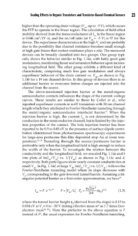
                       I ∝⋅   − /    F =  V / L  F =  42 m* (φ  ) 32  (1.5)
                                                             /
                              FF
                           F e
                               0
                       ds                ds     0     e 3    B
               where the tunnel barrier height φ (derived from the slope) is 0.13 to
                                            B
               0.034 eV at V = 0 to −30 V (taking effective mass m* as 1.7 times free-
                          g
               electron mass 80, 81 ). Here the prefactor in the above equation is  F
                         2
               instead of F , the usual expression for Fowler-Nordheim tunneling,

