
Page 42 - Organic Electronics in Sensors and Biotechnology
P. 42
Scaling Effects in Organic Transistors and Transistor-Based Chemical Sensors 19
Measurements stop here
10 –1
Mobility [cm 2 /(V·s)] 10 –3 44 K
–2
10
57 K
72 K
–4
10
92 K
125 K
10 –5 170 K
230 K
10 –6 290 K
0 200 400 600 800
sqrt (V /L) (V/cm) 1/2
ds
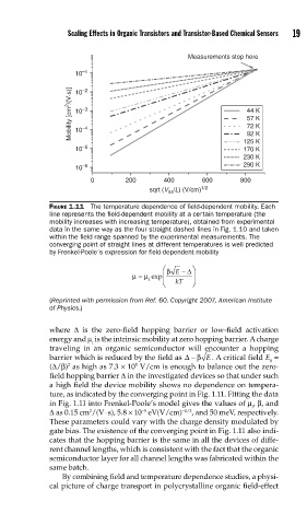
FIGURE 1.11 The temperature dependence of fi eld-dependent mobility. Each
line represents the fi eld-dependent mobility at a certain temperature (the
mobility increases with increasing temperature), obtained from experimental
data in the same way as the four straight dashed lines in Fig. 1.10 and taken
within the fi eld range spanned by the experimental measurements. The
converging point of straight lines at different temperatures is well predicted
by Frenkel-Poole’s expression for fi eld-dependent mobility
⎛ − ⎞
Δ
μ = μ exp ⎜ β E ⎟
i
⎝ kT ⎠
(Reprinted with permission from Ref. 60. Copyright 2007, American Institute
of Physics.)
where Δ is the zero-field hopping barrier or low-field activation
energy and μ is the intrinsic mobility at zero hopping barrier. A charge
i
traveling in an organic semiconductor will encounter a hopping
barrier which is reduced by the field as Δ− β E. A critical field E =
0
5
(Δ/β) as high as 7.3 × 10 V/cm is enough to balance out the zero-
2
field hopping barrier Δ in the investigated devices so that under such
a high field the device mobility shows no dependence on tempera-
ture, as indicated by the converging point in Fig. 1.11. Fitting the data
in Fig. 1.11 into Frenkel-Poole’s model gives the values of μ , β, and
i
2
−5
Δ as 0.15 cm /(V⋅ s), 5.8 × 10 eV(V/cm) −1/2 , and 50 meV, respectively.
These parameters could vary with the charge density modulated by
gate bias. The existence of the converging point in Fig. 1.11 also indi-
cates that the hopping barrier is the same in all the devices of diffe-
rent channel lengths, which is consistent with the fact that the organic
semiconductor layer for all channel lengths was fabricated within the
same batch.
By combining field and temperature dependence studies, a physi-
cal picture of charge transport in polycrystalline organic field-effect