
Page 45 - Organic Electronics in Sensors and Biotechnology
P. 45
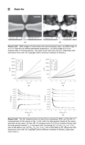
22    Chapter  One


                         (a)                            (b)

          FIGURE 1.13  SEM images of electrodes and semiconductor layer. (a) SEM image of
          a 5 nm channel just before pentacene evaporation. (b) SEM image of a 9 nm
          channel after I–V measurement. The white scale bars are 100 nm. (Reprinted with
          permission from Ref. 40. Copyright 2004, American Institute of Physics.)


             –600.0n
                                            –250.0n
                   V g  =                          V g  =
             –500.0n  0 V                            0 V
                     –6 V                   –200.0n  –6 V
             –400.0n  –12 V                         –12 V
                    –18 V                   –150.0n  –18 V
            I ds  (A)  –300.0n  –24 V      I ds  (A)  –100.0n  –24 V
                                                    –30 V
                    –30 V
             –200.0n
                                             –50.0n
             –100.0n
                                              0.0
               0.0
                  0            –1           –2            –3           –4            –5  0            –1            –2           –3   –4           –5
                           V ds  (V)                       V ds  (V)
                            (a)                            (b)
              –16.0                          –17.0
              –16.5
                                             –17.5
              –17.0
                                             –18.0
              –17.5                          –18.5
             ln (I ds /V ds )  –18.0        ln (I ds /V ds )  –19.0
              –18.5
              –19.0
              –19.5                          –19.5
                                             –20.0
              –20.0
                                             –20.5
              –20.5
                                             –21.0
                  0             1             2             3             4             5  0             1             2             3             4             5
                                                              –1
                               –1
                          |1/V ds | (V )                 |1/V ds | (V )
                            (c)                            (d)
          FIGURE 1.14  The DC characteristics of sub-10-nm pentacene FETs. (a) The DC I–V
          measurement of the device in Fig. 1.13b, with the side guards biased at the same
          potential as the drain. (b) The DC I–V measurement of a 19 nm channel device with
          the side guards biased; I /I increases with increasing |V |. (c) ln(I /V ) vs. 1/|V |
                             ds                     g      ds  ds     ds
          plot of the data in (a). (d) ln(I /V ) vs. 1/|V | plot of the data in (b). (Reprinted with
                                ds  ds    ds
          permission from Ref. 40. Copyright 2004, American Institute of Physics.) (See also
          color insert.)