
Page 40 - Organic Electronics in Sensors and Biotechnology
P. 40
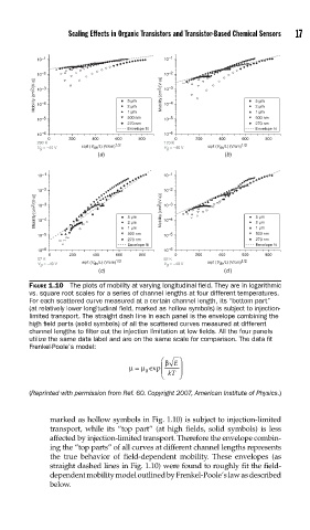
Scaling Effects in Organic Transistors and Transistor-Based Chemical Sensors   17


            10 –1                           10 –1
            10 –2                           10 –2
            Mobility [cm 2 /(V·s)]  10 –3  5 μm  Mobility [cm 2 /(V·s)]  10 –3  5 μm

                                            10 –4
            10 –4
                                   2 μm
                                                                   2 μm
                                   500 nm
                                                                   500 nm
            10 –5                  1 μm     10 –5                  1 μm
                                   270 nm                          270 nm
                                   Envelope fit                    Envelope fit
            10 –6                           10 –6
               0    200   400   600  800      0     200  400   600   800
            290 K      sqrt (V ds /L) (V/cm) 1/2  170 K  sqrt (V ds /L) (V/cm) 1/2
            V g  = –40 V                    V g  = –40 V
                           (a)                             (b)
            10 –1                           10 –1
            10 –2                           10 –2
            Mobility [cm 2 /(V·s)]  10 –3  5 μm  Mobility [cm 2 /(V·s)]  10 –3  5 μm

                                            10 –4
            10 –4
                                   2 μm
                                                                   2 μm
                                   500 nm
            10 –5                  1 μm     10 –5                  1 μm
                                                                   500 nm
                                   270 nm                          270 nm
                                   Envelope fit                    Envelope fit
            10 –6                           10 –6
               0    200   400   600   800     0     200  400   600   800
            57 K       sqrt (V ds /L) (V/cm) 1/2  92 K  sqrt (V ds /L) (V/cm) 1/2
            V g  = –40 V                    V g  = –40 V
                           (c)                             (d )
          FIGURE 1.10  The plots of mobility at varying longitudinal fi eld. They are in logarithmic
          vs. square root scales for a series of channel lengths at four different temperatures.
          For each scattered curve measured at a certain channel length, its “bottom part”
          (at relatively lower longitudinal fi eld, marked as hollow symbols) is subject to injection-
          limited transport. The straight dash line in each panel is the envelope combining the
          high fi eld parts (solid symbols) of all the scattered curves measured at different
          channel lengths to fi lter out the injection limitation at low fi elds. All the four panels
          utilize the same data label and are on the same scale for comparison. The data fi t
          Frenkel-Poole’s model:
                                           ⎛ β E  ⎞
                                   μ =  μ exp ⎜  ⎟
                                       0
                                           ⎝  kT  ⎠
          (Reprinted with permission from Ref. 60. Copyright 2007, American Institute of Physics.)

               marked as hollow symbols in Fig. 1.10) is subject to injection-limited
               transport, while its “top part” (at high fields, solid symbols) is less
               affected by injection-limited transport. Therefore the envelope combin-
               ing the “top parts” of all curves at different channel lengths represents
               the true behavior of field-dependent mobility. These envelopes (as
               straight dashed lines in Fig. 1.10) were found to roughly fit the field-
               dependent mobility model outlined by Frenkel-Poole’s law as described
               below.