
Page 35 - Organic Electronics in Sensors and Biotechnology
P. 35
12 Chapter One
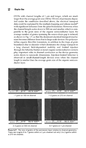
OTFTs with channel lengths of 1 μm and longer, which are much
larger than the average grain size (100 to 150 nm) of pentacene depos-
ited under the conditions described above, the electrical transport
data could be explained by the multiple trapping and release model 28
with significant influence from the grain boundaries. However, when
the channel length scales down to 500 nm and smaller, which is com-
parable to the grain sizes of the organic semiconductor layer, the
average number of grains spanning the source-drain gap is reduced,
as shown in Fig. 1.7, so that the dominant electrical transport mecha-
nism becomes different from that in large-scale devices. For polycrys-
talline organic thin-film transistors, in addition to the traps at grain
boundaries due to disorder which dominates the charge transport in
a long channel, field-dependent mobility and limited injection
through the Schottky barrier at metal-organic semiconductor contacts
play important roles in channel conduction as the device geometry
scales down to nanoscale dimensions. Injection-limited behavior is
observed in small-channel-length devices even when the channel
length is smaller than the average grain size of the organic semicon-
ductor layer.
~1 grain on 180 nm channel 1–2 grains on 270 nm channel
2–3 grains on 500 nm channel 6–7 grains on 1 μm channel
FIGURE 1.7 The size of grains of the pentacene layer relative to channel geometry.
There are roughly 6 to 7 grains within a 1 μm channel but only 1 to 2 grains within
a 270 nm channel.