
Page 30 - Organic Electronics in Sensors and Biotechnology
P. 30
Scaling Effects in Organic Transistors and Transistor-Based Chemical Sensors 7
SiO 2
+
n Si
Side Drain
Source guard Gate
SMU1 SMU2 SMU3
Semiconductor Parameter Analyzer SMU4
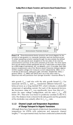
FIGURE 1.4 Three-dimensional device structure and circuit diagram for the
function of side guards in a nanoscale transistor used as chemical sensor.
To collect spreading currents traveling through the area outside the defi ned
channel, two side guards were designed on the two sides of the channel,
unconnected to and kept at the same potential as the drain. The three layers
from top are bottom-contact pentacene and Au/Ti electrodes (surface shown
+
by a SEM image of real device), SiO as dielectric, and n Si as gate. Each SMU
2
(source measurement unit) of the Semiconductor Parameter Analyzer (Agilent
4155C) supplies voltage and measures current independently. SMU1, 2, 3,
4 serves as the source, side-guard, gate, and drain, respectively. SMU1 =
ground; SMU3 = V ; SMU2 and SMU4 were set at the same value V .
g ds
(Reprinted with kind permission from Springer Scientifi c + Business Media. )
68
side guards (I ) and also with the side guards biased (I ). For
open ds
nanoscale devices, I and I manifested different behaviors. I
ds open open
behaved more as a long-channel FET, which indicates a substantial
component of spreading current. For each of the measured devices,
the maximum value of I was significantly lower than that of I
ds open
under the same voltage configuration, and the ratio I /I was
ds open
below 70%. This ratio was found to positively correlate to the W/L
ratio. The distance from a channel to its side guards and the geometry
of the electrodes may actually affect its I /I ratio.
ds open
1.1.3 Channel Length and Temperature Dependence
of Charge Transport in Organic Transistors
Although there have been reports of electrical characteristics at room
temperature for OTFTs with submicron and nanoscale channel
lengths, 37–40 no experimental study has been conducted systematically