
Page 27 - Organic Electronics in Sensors and Biotechnology
P. 27
4 Chapter One
H H H H
H H H H
H H H H
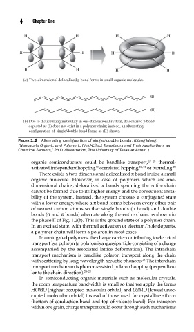
(a) Two-dimensional delocalized p bond forms in small organic molecules.
(I)
(II)
(b) Due to the resulting instability in one-dimensional system, delocalized p bond
depicted as (I) does not exist in a polymer chain; instead, an alternating
configuration of single/double bond forms as (II) shows.
FIGURE 1.2 Alternating confi guration of single/double bonds. (Liang Wang,
“Nanoscale Organic and Polymeric Field-Effect Transistors and Their Applications as
Chemical Sensors,” Ph.D. dissertation, The University of Texas at Austin.)
organic semiconductors could be bandlike transport, 17, 18 thermal-
19
activated independent hopping, correlated hopping, 20, 21 or tunneling. 22
There exists a two-dimensional delocalized π bond inside a small
organic molecule. However, in case of polymers which are one-
dimensional chains, delocalized π bonds spanning the entire chain
cannot be formed due to its higher energy and the consequent insta-
bility of the system. Instead, the system chooses a conjugated state
with a lower energy, where a π bond forms between every other pair
of nearest carbon atoms so that single bonds (σ bond) and double
bonds (σ and π bonds) alternate along the entire chain, as shown in
the phase II of Fig. 1.2(b). This is the ground state of a polymer chain.
In an excited state, with thermal activation or electron/hole dopants,
a polymer chain will form a polaron in most cases.
In conjugated polymers, the charge carrier contributing to electrical
transport is a polaron (a polaron is a quasiparticle consisting of a charge
accompanied by the associated lattice deformation). The intrachain
transport mechanism is bandlike polaron transport along the chain
23
with scattering by long-wavelength acoustic phonons. The interchain
transport mechanism is phonon-assisted polaron hopping (perpendicu-
lar to the chain direction). 24–25
In semiconducting organic materials such as molecular crystals,
the room temperature bandwidth is small so that we apply the terms
HOMO (highest occupied molecular orbital) and LUMO (lowest unoc-
cupied molecular orbital) instead of those used for crystalline silicon
(bottom of conduction band and top of valence band). For transport
within one grain, charge transport could occur through such mechanisms