
Page 29 - Organic Electronics in Sensors and Biotechnology
P. 29
6 Chapter One
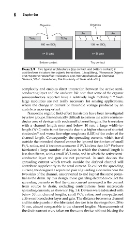
Organics Organics
Au Au
Ti/Au Ti/Au
100 nm SiO 2 100 nm SiO 2
n + Si gate n + Si gate
Bottom contact Top contact
FIGURE 1.3 Two typical architectures (top contact and bottom contact) in
upside-down structure for organic transistors. (Liang Wang, “Nanoscale Organic
and Polymeric Field-Effect Transistors and Their Applications as Chemical
Sensors,” Ph.D. dissertation, The University of Texas at Austin.)
complexity and enables direct interaction between the active semi-
conducting layer and the ambient. We note that some of the organic
semiconductors reported have a relatively high mobility. 10, 34 Such
large mobilities are not really necessary for sensing applications,
where the change in current or threshold voltage produced by an
analyte is more important.
Nanoscale organic field-effect transistors have been investigated
by a few groups. It is technically difficult to pattern the active semicon-
ductor area of devices with such small channel lengths. For transistors
with a channel length near and below 10 nm, a large width-to-
length (W/L) ratio is not favorable due to a higher chance of shorted
35
electrodes and worse line edge roughness (LER) of the order of the
channel length. Consequently, the spreading currents which travel
outside the intended channel cannot be ignored for devices of small
36
W/L ratios, and it becomes a concern if W/L is less than 10. We have
fabricated a large number of devices in which the channel length is
less than 50 nm, with a small W/L ratio, and in which the active semi-
conductor layer and gate are not patterned. In such devices the
spreading current which travels outside the defined channel will
contribute significantly to the total current. To collect the spreading
current, we designed a separated pair of guarding electrodes near the
two sides of the channel, unconnected to and kept at the same poten-
tial as the drain. By this design, these guarding electrodes collect the
spreading currents so that the drain current measured is the current
from source to drain, excluding contributions from macroscale
spreading currents, as shown in Fig. 1.4. Devices were fabricated with
below 50 nm channel lengths, small W/L ratios, and non-patterned
active semiconductor layer and gate. The distance between a channel
and its side guards in the fabricated devices is in the range from 20 to
50 nm, almost comparable to the channel lengths. Measurements of
the drain current were taken on the same device without biasing the