
Page 33 - Organic Electronics in Sensors and Biotechnology
P. 33
10 Chapter One
0 V –15.0 0 V
–10.0 290 K 290 K
–8 V –8 V
–16 V 5 μm –10.0 –16 V 270 nm
Drain current I d (μA) –6.0 V side = V ds Drain current I d (μA) –5.0 V side = V ds
–8.0
–24 V
–24 V
–32 V
–32 V
–40 V
–40 V
–4.0
–2.0
0.0
0.0
0 –5 –10 –15 –20 –25 –30 –35 –40 0 –5 –10 –15 –20
V ds (V) V ds (V)
(a) (b)
0 V –14.0 0 V
–8 V 57 K –8 V 57 K
–15.0 –16 V 5 μm –12.0 –16 V 270 nm
Drain current I d (nA) –10.0 V side = V ds Drain current I d (μA) –8.0 V side = V ds
–24 V
–24 V
–10.0
–32 V
–32 V
–40 V
–40 V
–6.0
–5.0
–4.0
–2.0
0.0
0.0
0 –5 –10 –15 –20 –25 –30 –35 –40 0 –5 –10 –15 –20
V ds (V) V ds (V)
(c) (d)
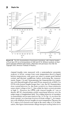
FIGURE 1.5 The DC characteristics of pentacene transistors, with channel lengths
of 5 μm and 270 nm at temperatures of 290 and 57 K. Different symbols on each
panel represent different gate biases. (Reprinted with permission from Ref. 60.
Copyright 2007, American Institute of Physics.)
channel lengths were measured with a semiconductor parameter
analyzer in mTorr vacuum from room temperature down to liquid
helium temperatures, with great care taken to ensure good thermal
contact and thermal equilibrium before performing the measure-
ments. Figure 1.5a and b demonstrates the characteristics for transis-
tors with channel length of 5 μm and 270 nm, respectively, at 290 K. For
OTFTs with channel lengths longer than 1 μm, the DC characteristics
show normal behavior; i.e., the drain current is in a linear relation to
source-drain voltage at low V bias while the drain current saturates
ds
at high V . However, for OTFTs with channel lengths of 1 μm or
ds
shorter, the DC characteristics exhibit superlinear behavior over the
entire range of longitudinal field. This scaling behavior of transition
in characteristic can be seen clearly in Fig. 1.6. In Fig. 1.6, we show the
drain current I as a function of source-to-drain voltage V for transis-
d ds
tors with different channel lengths at room temperature. Because the
W/L ratios of all channels were kept at the same value of 10 in fabri-
cation, this figure demonstrates charge transport scaling behavior in