
Page 36 - Organic Electronics in Sensors and Biotechnology
P. 36
Scaling Effects in Organic Transistors and Transistor-Based Chemical Sensors 13
10 –1 10 –1
10 –2 10 –2
10 –3 10 –3
Ohmic 10 –4
I ds /W (A/cm) 10 –5 5 μm I ds /W (A/cm) 10 –5 Ohmic 5 μm
10 –4
2 μm
2 μm
1 μm
1 μm
10 –6
500 nm
270 nm 10 –6 500 nm
270 nm
10 –7 180 nm 10 –7 180 nm
130 nm 130 nm
10 –8 100 nm 10 –8 100 nm
80 nm 80 nm
290 K 10 4 10 5 10 6 125 K 10 4 10 5 10 6
V g = –40 V V g = –40 V
V ds /L (V/cm) V ds /L (V/cm)
10 –1 10 –1
5 μm 5 μm
2 μm 2 μm
10 –2 1 μm 10 –2 1 μm
500 nm 500 nm
10 –3 270 nm 10 –3 270 nm
180 nm 10 –4 180 nm
10 –4
I ds /W (A/cm) 10 –5 100 nm I ds /W (A/cm) 10 –5 100 nm
130 nm
130 nm
80 nm
80 nm
10 –6
10 –6
10 –7 Ohmic 10 –7 Ohmic
10 –8 10 –8
57 K 10 4 10 5 10 6 4.8 K 10 4 10 5 10 6
V g = –40 V V g = –40 V
V ds /L (V/cm) V ds /L (V/cm)
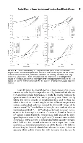
FIGURE 1.8 The current density vs. longitudinal fi eld plots for various channel
lengths at four different temperatures. The solid lines in these plots are the ohmic
channel transport currents, calculated based on the mobility extracted from long-
channel (5 μm) devices. These lines serve as the references to investigate the
issues of contact injection-limited transport and fi eld-dependent mobility. All the four
fi gures are exactly on the same scale for the purpose of comparison. (See also color
insert.)
Figure 1.8 shows the scaling behavior of charge transport in organic
transistors, including field-dependent mobility, injection-limited trans-
port, and temperature dependence. To study the scaling behavior, the
apparent contribution of the device geometry was filtered out by
taking the current density vs. longitudinal field and plotting that
relation for various channel lengths at four different temperatures,
under a certain high gate bias beyond the threshold voltage of the
transistors (−40 V). The solid lines in these plots are the ohmic channel
transport currents at V =−40 V calculated through the drain-current
g
equation for linear-region operation of transistors, based on the mobi-
lity values extracted from the measurement data taken at the corre-
sponding temperature on the long-channel (5 μm) devices where field
dependence of the mobility is not significant at its operative longitu-
dinal field and the channel resistance is much larger than contact
resistance. At the same temperature, for all the devices with different
channel lengths, their calculated ohmic channel transport behaviors,
ignoring other factors, should fall onto the same solid line on the