
Page 34 - Organic Electronics in Sensors and Biotechnology
P. 34
Scaling Effects in Organic Transistors and Transistor-Based Chemical Sensors 11
–25.0 5 μm (1)
2 μm (2)
4
–20.0 1 μm (3) 3
500 nm (4)
270 nm (5) 2
–15.0
I ds (μA) 5
–10.0
1
–5.0
0.0
290 K 0 –10 –20 –30 –40
V = –40 V V (V)
g
ds
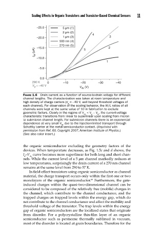
FIGURE 1.6 Drain current as a function of source-to-drain voltage for different
channel lengths. The characterization was taken at room temperature and
high density of charge carriers (V =−40 V, well beyond threshold voltages of
g
each channel). For observation of the scaling behavior, the W/L ratios of all
channels were kept at the same value of 10 in fabrication to exclude
geometric factors. Clearly in the regime of V < V − V , the current-voltage
ds g th
characteristic transitions from linear to superlinear upon scaling from micron
to submicron channel length. For submicron channels there is an exponential
dependence at very small V due to the injection-limited transport through
ds
Schottky barrier at the metal-semiconductor contact. (Reprinted with
permission from Ref. 60. Copyright 2007, American Institute of Physics.)
(See also color insert.)
the organic semiconductor excluding the geometry factors of the
devices. When temperature decreases, as Fig. 1.5c and d shows, the
I –V curve becomes more superlinear for both long and short chan-
d ds
nels. While the current level of a 5 μm channel markedly reduces at
low temperatures, surprisingly the drain current of a 270 nm channel
remains at the same level from 290 to 57 K.
In field-effect transistors using organic semiconductor as channel
material, the charge transport occurs only within the first one or two
monolayers of the organic semiconductor. Furthermore, the gate-
49
induced charges within the quasi-two-dimensional channel can be
considered to be composed of the relatively free (mobile) charges in
the channel, which contribute to the channel conductance, and the
trapped charges on trapped levels within the energy gap, which do
not contribute to the channel conductance and affect the mobility and
threshold voltage of the transistor. The trap levels within the energy
gap of organic semiconductors are the localized states that originate
from disorder. For a polycrystalline thin-film layer of an organic
semiconductor such as pentacene thermally sublimed in vacuum,
most of the disorder is located at grain boundaries. Therefore for the