
Page 53 - Organic Electronics in Sensors and Biotechnology
P. 53
30 Chapter One
so that the weight of influence of grain boundaries on electrical trans-
port and chemical sensing reduces and other factors become more
important. At smaller channel dimensions, especially when the chan-
nel length is comparable to or smaller than the grain size of polycrys-
talline organic molecules or conjugated polymers, we might possibly
observe the electrical transport and chemical sensing behaviors within
the body of grains which may exhibit a mechanism different from that
in large-scale devices where grain boundaries dominate. In addition,
contact barrier at the interface between electrode and semiconductor
will play an important role in scaling since the resistance through the
semiconductor channel becomes smaller. We believe it is the injection
of current at the source/drain contacts that gets modulated by the
116
analyte molecules. Thus the behavior of nanoscale OFET sensors is
markedly different from that of larger-channel-length devices.
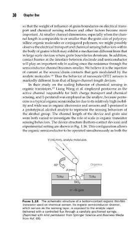
In their study on the scaling behavior of chemical sensing in
115
organic transistors, Liang Wang et al. employed pentacene as the
active channel responsible for both charge transport and chemical
sensing, and 1-pentanol was employed as the analyte, because penta-
cene is a typical organic semiconductor due to its relatively high mobil-
ity and wide use in organic electronics and sensors and 1-pentanol is
a prototypical alcohol analyte to represent the sensing behaviors of
the alcohol group. The channel length of the device and grain size
were both varied to investigate the role of scale in organic transistor
sensing behaviors. The device structure (bottom-contact devices) and
experimental setting are shown in Fig. 1.16. This configuration allows
the organic semiconductor to be operated simultaneously as both the
V (mL/min), analyte molecules
60° Organics
d (mm)
Ti/Au Ti/Au
SiO 2
n + –Si gate
FIGURE 1.16 The schematic structure of a bottom-contact organic thin-fi lm
transistor used as chemical sensor. Its organic semiconductor channel,
which serves as the sensing layer, is exposed to the analyte vapor
delivered with a controlled fl ux through a carefully positioned syringe.
(Reprinted with kind permission from Springer Science and Business Media
from Ref. 68)