
Page 58 - Organic Electronics in Sensors and Biotechnology
P. 58
Scaling Effects in Organic Transistors and Transistor-Based Chemical Sensors 35
(a) (b)
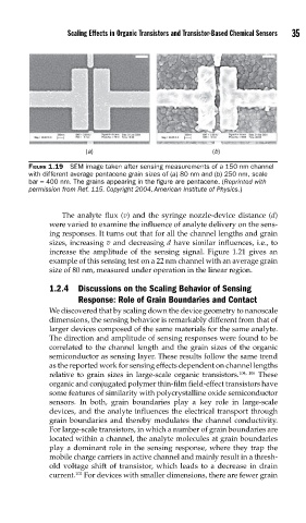
FIGURE 1.19 SEM image taken after sensing measurements of a 150 nm channel
with different average pentacene grain sizes of (a) 80 nm and (b) 250 nm, scale
bar = 400 nm. The grains appearing in the fi gure are pentacene. (Reprinted with
permission from Ref. 115. Copyright 2004, American Institute of Physics.)
The analyte flux (v) and the syringe nozzle-device distance (d)
were varied to examine the influence of analyte delivery on the sens-
ing responses. It turns out that for all the channel lengths and grain
sizes, increasing v and decreasing d have similar influences, i.e., to
increase the amplitude of the sensing signal. Figure 1.21 gives an
example of this sensing test on a 22 nm channel with an average grain
size of 80 nm, measured under operation in the linear region.
1.2.4 Discussions on the Scaling Behavior of Sensing
Response: Role of Grain Boundaries and Contact
We discovered that by scaling down the device geometry to nanoscale
dimensions, the sensing behavior is remarkably different from that of
larger devices composed of the same materials for the same analyte.
The direction and amplitude of sensing responses were found to be
correlated to the channel length and the grain sizes of the organic
semiconductor as sensing layer. These results follow the same trend
as the reported work for sensing effects dependent on channel lengths
relative to grain sizes in large-scale organic transistors. 104, 106 These
organic and conjugated polymer thin-film field-effect transistors have
some features of similarity with polycrystalline oxide semiconductor
sensors. In both, grain boundaries play a key role in large-scale
devices, and the analyte influences the electrical transport through
grain boundaries and thereby modulates the channel conductivity.
For large-scale transistors, in which a number of grain boundaries are
located within a channel, the analyte molecules at grain boundaries
play a dominant role in the sensing response, where they trap the
mobile charge carriers in active channel and mainly result in a thresh-
old voltage shift of transistor, which leads to a decrease in drain
current. For devices with smaller dimensions, there are fewer grain
102