
Page 60 - Organic Electronics in Sensors and Biotechnology
P. 60
Scaling Effects in Organic Transistors and Transistor-Based Chemical Sensors 37
22 nm channel
1.6
Normalized drain current 1.2
1.4
1.0
Reference
0.8
d = 2 mm
d = 4 mm
0.6 d = 5 mm
0 10 20 30 40 50 60
Time (s)
(a)
(b)
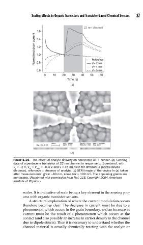
FIGURE 1.21 The effect of analyte delivery on nanoscale OTFT sensor. (a) Sensing
data of a pentacene transistor of 22 nm channel in response to 1-pentanol, with
V =−2 V, V = V =−0.4 V and v = 45 mL/min for different d (nozzle-device
g ds side
distance), reference = absence of analyte. (b) SEM image of the device in (a) taken
after measurements, grain ~80 nm, scale bar = 100 nm. The appearing grains are
pentacene. (Reprinted with permission from Ref. 115. Copyright 2004, American
Institute of Physics.)
scales. It is indicative of scale being a key element in the sensing pro-
cess with organic transistor sensors.
A structural explanation of where the current modulation occurs
therefore becomes clear. The decrease in current must be due to a
phenomenon which occurs in the grain boundary, and an increase in
current must be the result of a phenomenon which occurs at the
contact (and also possibly an increase in carrier density in the channel
due to dipole effects). Then it is necessary to understand whether the
channel material is actually chemically reacting with the analyte or