
Page 64 - Organic Electronics in Sensors and Biotechnology
P. 64
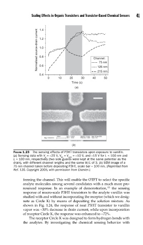
Scaling Effects in Organic Transistors and Transistor-Based Chemical Sensors   41


                        1.4
                       Normalized source-drain current  1.2  Channel:


                        1.0


                        0.8
                                                        75 nm
                        0.6
                                                        215 nm
                        0.4                             125 nm
                             0    10     20    30    40    50
                                          Time (s)
                                           (a)


                                          (b)

          FIGURE 1.23  The sensing effects of P3HT transistors upon exposure to vanillin.
          (a) Sensing data with V =−25 V, V = V  =−10 V, and −15 V for L < 100 nm and
                           g        ds  side
          L > 100 nm, respectively (two side guards were kept at the same potential as the
          drain), with different channel lengths and the same W/L of 3. (b) SEM image of a
          75 nm channel taken before depositing P3HT, scale bar = 100 nm. (Reprinted from
          Ref. 130. Copyright 2005, with permission from Elsevier.)

               forming the channel. This will enable the OTFT to select the specific
               analyte molecules among several candidates with a much more pro-
                                                             122
               nounced response. In an example of demonstration,  the sensing
               response of macro-scale P3HT transistors to the analyte vanillin was
               studied with and without incorporating the receptor (which we desig-
               nate as Circle K) by means of depositing the solution mixture. As
               shown in Fig. 1.24, the response of neat P3HT transistor to vanillin
               vapor was ~30% decrease in drain current, while upon incorporation
               of receptor Circle K, the response was enhanced to ~72%.
                   The receptor Circle K was designed to form hydrogen bonds with
               the analytes. By investigating the chemical sensing behavior with