
Page 67 - Organic Electronics in Sensors and Biotechnology
P. 67
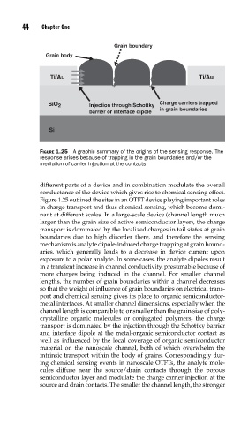
44    Chapter  One

                                      Grain boundary
                 Grain body


                   Ti/Au              +          +               Ti/Au
                                      +          +

                  SiO 2        Injection through Schottky   Charge carriers trapped
                               barrier or interface dipole   in grain boundaries


                  Si


               FIGURE 1.25  A graphic summary of the origins of the sensing response. The
               response arises because of trapping in the grain boundaries and/or the
               mediation of carrier injection at the contacts.


               different parts of a device and in combination modulate the overall
               conductance of the device which gives rise to chemical sensing effect.
               Figure 1.25 outlined the sites in an OTFT device playing important roles
               in charge transport and thus chemical sensing, which become domi-
               nant at different scales. In a large-scale device (channel length much
               larger than the grain size of active semiconductor layer), the charge
               transport is dominated by the localized charges in tail states at grain
               boundaries due to high disorder there, and therefore the sensing
               mechanism is analyte dipole-induced charge trapping at grain bound-
               aries, which generally leads to a decrease in device current upon
               exposure to a polar analyte. In some cases, the analyte dipoles result
               in a transient increase in channel conductivity, presumable because of
               more charges being induced in the channel. For smaller channel
               lengths, the number of grain boundaries within a channel decreases
               so that the weight of influence of grain boundaries on electrical trans-
               port and chemical sensing gives its place to organic semiconductor-
               metal interfaces. At smaller channel dimensions, especially when the
               channel length is comparable to or smaller than the grain size of poly-
               crystalline organic molecules or conjugated polymers, the charge
               transport is dominated by the injection through the Schottky barrier
               and interface dipole at the metal-organic semiconductor contact as
               well as influenced by the local coverage of organic semiconductor
               material on the nanoscale channel, both of which overwhelm the
               intrinsic transport within the body of grains. Correspondingly dur-
               ing chemical sensing events in nanoscale OTFTs, the analyte mole-
               cules diffuse near the source/drain contacts through the porous
               semiconductor layer and modulate the charge carrier injection at the
               source and drain contacts. The smaller the channel length, the stronger