
Page 62 - Organic Electronics in Sensors and Biotechnology
P. 62
Scaling Effects in Organic Transistors and Transistor-Based Chemical Sensors 39
110
carbon chains. Therefore, in addition to the polar nature of analyte
molecules, sensing response could be adjusted with the use of polar
110
vs. nonpolar side chain moieties of the organic semiconductor. For
instance, ethanol showed no electrical response with the nonpolar
side chain but did show a response with the polar side chain. This
was most likely due to a poor interaction of the short ethanol alkyl
chain to the nonpolar side chain and a much better interaction of the
polar ethanol to the polar side chain.
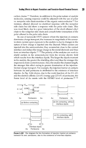
In case of nanoscale OTFT sensors where the injection at contacts
dominates charge transport, the increases in magnitude of the source-
to-drain current upon exposure to the analyte is due to changes in the
nature of how charge is injected into the channel. When carriers are
injected into the semiconductor, they accumulate close to the contact
interface and induce the image charge in the metal electrode and thus
form an interface dipole. 123, 124 The polarity of the analytes can work to
shield carriers in the semiconductor from the reverse electric field
which results from the interface dipole. The larger the dipole moment
in the analyte, the greater the shielding effect and thus the stronger the
response in drain-current increase. Also, the smaller the channel length,
the stronger this effect owing to greater domination of the injection-
limited charge transport. For example, the injection barrier at contacts
between Au and pentacene is attributed to the existence of interface
dipoles. As Fig. 1.22a shows, due to the work function of Au (5.1 eV)
and the electron affinity (2.6 eV)/energy gap (2.5 eV) of pentacene, the
Fermi level of Au meets with the HOMO level of pentacene. 125, 126
E vac
2.6 eV
LUMO
5.1 eV
2.5 eV
HOMO
Au Pentacene Au Au Pentacene Au
(b) On contacting, without
(a) Before contacting.
interface dipole.
Δ
(c) On contacting, with
interface dipole.
Δ
– + + –
Interface dipole
Au Pentacene Au
FIGURE 1.22 The diagram for the formation of injection barrier at contacts
between Au and pentacene, due to the existence of interface dipoles.