
Page 59 - Organic Electronics in Sensors and Biotechnology
P. 59
36 Chapter One
1.2
Grain ~ 140 nm
1.0
Normalized drain current 0.8 2 μm
0.6
4 μm
0.4
6 μm
0.2 12 μm
36 μm
0.0
0 10 20 30 40 50 60
Time (s)
(a)
1.2 Grain ~ 1 μm
Normalized drain current 0.8 2 μm
1.0
0.6
4 μm
0.4
6 μm
0.2 12 μm
36 μm
0.0
0 10 20 30 40 50 60
Time (s)
(b)
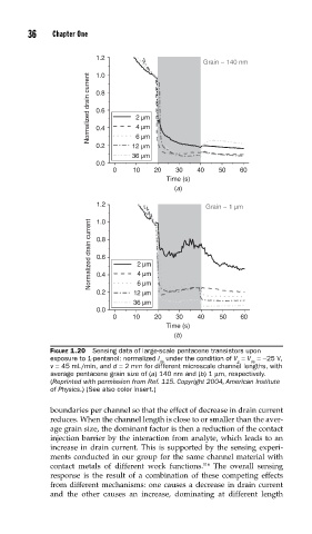
FIGURE 1.20 Sensing data of large-scale pentacene transistors upon
exposure to 1-pentanol: normalized I under the condition of V = V =−25 V,
ds g ds
v = 45 mL/min, and d = 2 mm for different microscale channel lengths, with
average pentacene grain size of (a) 140 nm and (b) 1 μm, respectively.
(Reprinted with permission from Ref. 115. Copyright 2004, American Institute
of Physics.) (See also color insert.)
boundaries per channel so that the effect of decrease in drain current
reduces. When the channel length is close to or smaller than the aver-
age grain size, the dominant factor is then a reduction of the contact
injection barrier by the interaction from analyte, which leads to an
increase in drain current. This is supported by the sensing experi-
ments conducted in our group for the same channel material with
116
contact metals of different work functions. The overall sensing
response is the result of a combination of these competing effects
from different mechanisms: one causes a decrease in drain current
and the other causes an increase, dominating at different length