
Page 12 - Photodetection and Measurement - Maximizing Performance in Optical Systems
P. 12
Photodetection Basics
Photodetection Basics 5
For another detection demonstration, find a piece of silicon, connect it to the ground
terminal of a laboratory oscilloscope and press a 10-MW probe against the top surface.
Illuminate the contact point with a bright red LED modulated at 1kHz. You should
see a strong response on the scope display. This “cat’s whisker” photodetector is about
as simple a demonstration of photodetection as I can come up with! This isn’t a semi-
conductor pn-junction diode, but a metal-semiconductor diode like a Schottky diode.
It seems that almost any junction between dissimilar conducting materials will
operate as a photodetector, including semiconductors, metals, electrolytes, and more
fashionably organic semiconductors.
1.4 Real Fabrications
Although all pn-junction diodes are photosensitive, and a diode can be formed
by pressing together two different semiconductor (or metal and semiconductor)
materials in the manner of the first cat’s whisker radio detectors or the
previous TRY IT! demonstrations, for optimum and repeatable performance we
usually turn to specially designed structures, those commercially produced.
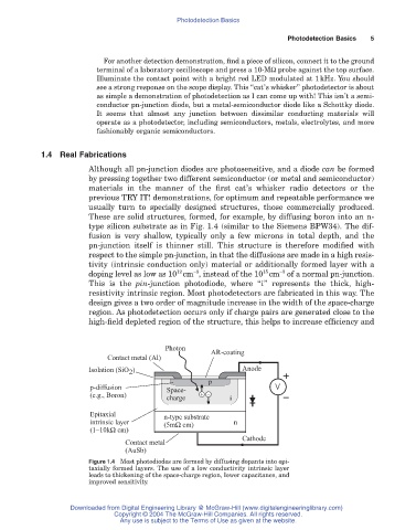
These are solid structures, formed, for example, by diffusing boron into an n-
type silicon substrate as in Fig. 1.4 (similar to the Siemens BPW34). The dif-
fusion is very shallow, typically only a few microns in total depth, and the
pn-junction itself is thinner still. This structure is therefore modified with
respect to the simple pn-junction, in that the diffusions are made in a high resis-
tivity (intrinsic conduction only) material or additionally formed layer with a
-3
12
15
-3
doping level as low as 10 cm , instead of the 10 cm of a normal pn-junction.
This is the pin-junction photodiode, where “i” represents the thick, high-
resistivity intrinsic region. Most photodetectors are fabricated in this way. The
design gives a two order of magnitude increase in the width of the space-charge
region. As photodetection occurs only if charge pairs are generated close to the
high-field depleted region of the structure, this helps to increase efficiency and
Photon
AR-coating
Contact metal (Al)
Isolation (SiO ) Anode
2
p
p-diffusion Space- V
(e.g., Boron)
charge i
Epitaxial n-type substrate
intrinsic layer (5mW cm) n
(1–10kW cm)
Cathode
Contact metal
(AuSb)
Figure 1.4 Most photodiodes are formed by diffusing dopants into epi-
taxially formed layers. The use of a low conductivity intrinsic layer
leads to thickening of the space-charge region, lower capacitance, and
improved sensitivity.
Downloaded from Digital Engineering Library @ McGraw-Hill (www.digitalengineeringlibrary.com)
Copyright © 2004 The McGraw-Hill Companies. All rights reserved.
Any use is subject to the Terms of Use as given at the website.