
Page 9 - Photodetection and Measurement - Maximizing Performance in Optical Systems
P. 9
Photodetection Basics
2 Chapter One
Space- Electric
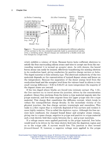
(a) Before Contacting (b) After Contacting
charge field
Acceptor doping (e.g., B) density
p
p
A
Depletion Region
n K
n
Diffusion-driven
Donor doping Field-driven
(e.g., As,P)
Bound Free
Figure 1.1 The pn-junction. The presence of predominately different polarities
of free carriers in the two contacted materials leads to asymmetrical conduc-
tivity, a rectifying action. Bound charges are indicated by a double circle and
free charges by a single circle.
which exhibits a valency of three. Because boron lacks sufficient electrons to
satisfy the four surrounding silicon atoms and tries to accept one from the sur-
rounding material it is termed an acceptor atom. As with donors, the bound
boron atoms can easily be ionized, effectively transferring the missing electron
to its conduction band, giving conduction by positive charge carriers or holes.
The doped material is then termed p-type. The electrical conductivity of the two
materials depends on the concentration of ionized dopant atoms and hence on
the temperature. Because the separation of the donor energy level from the
conduction band and the acceptor level from the valence band in silicon is very
small (energy difference ª 0.02 to 0.05eV) at room temperature the majority of
the dopant atoms are ionized.
If the two doped silicon blocks are forced into intimate contact (Fig. 1.1b),
the free carriers try to travel across the junction, driven by the concentration
gradient. Hence free electrons from the lower n-type material migrate into the
p-type material, and free holes migrate from the upper p-type into the n-type
material. This charge flow constitutes the diffusion current, which tends to
reduce the nonequilibrium charge density. In the immediate vicinity of the
physical junction, the free charge carriers intermingle and recombine. This
leads to a thin region that is relatively depleted of free carriers and renders it
more highly resistive. This is called the depletion region. Although the free car-
riers have combined, the charged bound donor and acceptor atoms remain,
giving rise to a space charge, negative in p-type and positive in n-type material
and a real electric field then exists between the n- and p-type materials.
If a voltage source were applied positively to the p-type material, free holes
would tend to be driven by the total electric field into the depletion region and
on to the n-type side. A current would flow. The junction is then termed
forward-biased. If, however, a negative voltage were applied to the p-type
Downloaded from Digital Engineering Library @ McGraw-Hill (www.digitalengineeringlibrary.com)
Copyright © 2004 The McGraw-Hill Companies. All rights reserved.
Any use is subject to the Terms of Use as given at the website.