Page 33 - Power Electronics Handbook
P. 33
26   Power semiconductor devices

                       generated at the base-emitter junction are gathered up by the collector, so
                       that increasing V,   does not appreciably affect IC. This is known as the
                       saturation region of the characteristic. The larger the value of base current,
                       the higher the collector current at which saturation occurs. Therefore a
                       bipolar transistor is  essentially a current-operated device. At very large
                       values  of  VcE  the  carriers  attain sufficient energy to  cause  avalanche
                       breakdown.
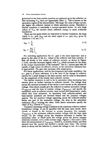
                         There are two gains which are important in bipolar transistors, the large
                       signal or  d.c.  gain (hm)  and the small signal or a.c.  gain  (h&  given by
                       equations (1.6)  and (1.7).


                         For switching applications the d.c. gain is the most  important, and is
                       given by the ratio of  the d.c.  values of  the collector and base currents. It
                       falls off  slowly  at  low  values of  collector current, as  shown in  Figure
                       l.ll(d), and also increases slightly with VcE, which accounts for the slope
                       in the output characteristic of the transistor. The d.c. current gain falls off
                       rapidly at high values of collector current, as the saturation resistance line
                       is approached. The gain also increases with temperature.
                         For linear applications, and for low-frequency and audio amplifiers, the
                       a.c.  gain  is of  more relevance. It is the ratio of  the change in collector
                       current for a small change in the base current, and its value is determined
                       by the magnitude of  the steady state collector current.
                         The bipolar transistor is said to be in saturation when increasing base
                       current gives no further increase in collector current. The voltage drop
                       across the external terminals of the device is now known as the saturation
                       voltage. Data sheets usually give the collector to emitter saturation voltage
                       (V,sA,)   and the base to emitter voltage  (VBE(SAT)), and specify the
                       conditions, such as collector current, base current and temperature, under
                       which  they  were  measured.  At  saturation  both  collector-emitter and
                       base-emitter  junctions  are  forward  biased  and  the  junction  voltages
                       oppose. The net junction voltage appearing across the collector-emitter
                       forms  one  part  of  the  saturation  voltage, the  drop  in  the  saturation
                       resistance (Ra) forming the other.  Data sheets sometimes specify  the
                       value of  RCE instead of  V-(sAm.
                         Transistor sustaining voltage is defined as the minimum collector-emitter
                       breakdown voltage. It can be specified with the base open circuit, short
                       circuit,  or  biased  in  the  forward  or  reverse  directions.  For  example,
                       V,?(S"S)  is the minimum collector-emitter voltage with the base open
                       circuit.  As  the  voltage  across  the  transistor  increases  it  reaches  the
                       sustaining value,  at which  point  the  voltage  across the device remains
                       relatively constant, over a wide current range. Figures 1.12(a) and 1.12(b)
                       show the measurement of  VcEo(sus).  Switch S,  is initially closed, and then
                       opened once the current has reached a steady state value. The current
                       starts to decay and the inductor L1 causes the voltage to rise. At a voltage

