
Page 38 - Power Electronics Handbook
P. 38
Unipolar transistors 3 1
Base Emitter
contact contact
-type emitter
Base
Emitter Base
Emitter metal
I
Base metal
n+ substrate
I
Collector
(b) metal
Emitter Base
p+ diffusion
n substrate
n+ substrate n+ diffusion
(d) Collector 1
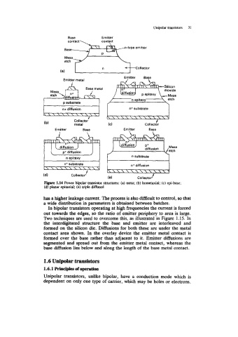
Figure 1.14 Power bipolar transistor structures: (a) mesa; (b) hornetaxial; (c) epi-base;
(d) planar epitaxial; (e) triple diffused
has a higher leakage current. The process is also difficult to control, so that
a wide distribution in parameters is obtained between batches.
In bipolar transistors operating at high frequencies the current is forced
out towards the edges, so the ratio of emitter periphery to area is large.
Two techniques are used to overcome this, as illustrated in Figure 1.15. In
the interdigitated structure the base and emitter are interleaved and
formed on the silicon die. Diffusions for both these are under the metal
contact area shown. In the overlay device the emitter metal contact is
formed over the base rather than adjacent to it. Emitter diffusions are
segmented and spread out from the emitter metal contact, whereas the
base diffusion lies below and along the length of the base metal contact.
1.6 Unipdar transistorS
1.6.1 R.iadpks doperation
Unipolar transistors, unlike bipolar, have a conduction mode which is
dependent on only one type of carrier, which may be holes or electrons.