
Page 42 - Power Electronics Handbook
P. 42
Unipolar transistors 35
Increasing drain-source voltage causes a rise in the drain current.
However, the resulting increase in the voltage drop causes a reduction in
the channel conductivity. This reduction has the same effect as a
constriction in the inversion layer, resulting in a knee in the curves of
Figure 1.18(b). When the drain-source and gate-source voltages are equal
the voltage between the gate and drain ends of the channel is zero and this
is the pinchsff condition (V-1). Further increase in the drain-source
voltage causes the drain depletion layer to increase and the end of the
channel to move towards the source. The drain current is kept substantially
constant by the electrons being swept through the depletion layer.
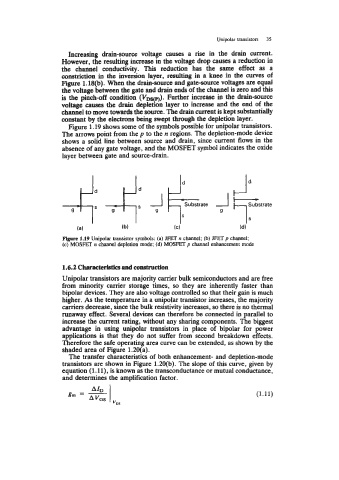
Figure 1.19 shows some of the symbols possible for unipolar transistors.
The arrows point from the p to the n regions. The depletion-mode device
shows a solid line between source and drain, since current flows in the
absence of any gate voltage, and the MOSFET symbol indicates the oxide
.&:
layer between gate and source-drain.
4
'I:"""'"'
4; a t e +
G
r
s
(a) (b) (C) (d)
Figure 1.19 Unipolar transistor symbols: (a) IFET n channel; (b) JFET p channel;
(c) MOSFET n channel depletion mode; (d) MOSFET p channel enhancement mode
1.6.2 Characteristies and construction
Unipolar transistors are majority carrier bulk semiconductors and are free
from minority carrier storage times, so they are inherently faster than
bipolar devices. They are also voltage controlled so that their gain is much
higher. As the temperature in a unipolar transistor increases, the majority
carriers decrease, since the bulk resistivity increases, so there is no thermal
runaway effect. Several devices can therefore be connected in parallel to
increase the current rating, without any sharing components. The biggest
advantage in using unipolar transistors in place of bipolar for power
applications is that they do not suffer from second breakdown effects.
Therefore the safe operating area curve can be extended, as shown by the
shaded area of Figure 1.20(a).
The transfer characteristics of both enhancement- and depletion-mode
transistors are shown in Figure 1.20(b). The slope of this curve, given by
equation (l.ll), is known as the transconductance or mutual conductance,
and determines the amplification factor.
(1.11)