
Page 43 - Power Electronics Handbook
P. 43
36 Power semiconductor devices
IC or ID
E\ Maximum
,Maximum
voltage
L I fi
vCE Or vDS
/
- w +
VGS "OS
(b)
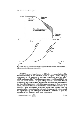
Figme 1.20 Unipolar transistor characteristics: (a) safe operating area and comparison with a
bipolar transistor; (b) transfer characteristic
MOSFETs are used in preference to JFETs for power applications. The
breakdown voltage of this structure, shown in Figure l.l8(a), is largely
determined by the thickness of the oxide between the gate and drain,
which can be quite thin. Vertical structures, as shown in Figure 1.21(a), are
used for power devices. The gate voltage creates a horizontal channel
between the two source regions, which results in an inversion layer down to
the drain. The figure shows a plysilicon gate arrangement. Once inversion
occurs, the device behaves as a non-linear resistor and not as an n-p-n
transistor. This arrangement gives high breakdown voltages, but the
capacitance between drain and gate is relatively large, so it is not very good
for high-frequency use. The figure of merit of a transistor is given by
equation (1.12), where Ci, is the input capacitance.
Figure of merit = - (1.12)
gm
Cin